Light emitting diode

a diode and light-emitting technology, applied in the direction of basic electric elements, electrical equipment, semiconductor devices, etc., can solve the problems of insufficient color rendering index (cri), excessive total volume of packages, and decrease of package yield

Inactive Publication Date: 2012-02-09
ADVANCED OPTOELECTRONICS TECH
View PDF6 Cites 9 Cited by
  • Summary
  • Abstract
  • Description
  • Claims
  • Application Information

AI Technical Summary

Benefits of technology

[0021]As disclosed, the fluorescent conversion layer covering the surface of the light emitting diode to obtain light mixed as white light can minimize the capacity of the package, and the disclosure of the light emitting diode has multiple wavelength regions, avoiding the different lifetimes between chips and enhancing efficiency of package. As well, the different wavelengths on the light emitting diode can be mixed better than R, G, B chips, because of distances between the chips.

Problems solved by technology

Although the blue chip with yellow phosphor package can generate white light, the color rendering index (CRI) is insufficient, especially in the red spectrum range, being less than other ranges, such as yellow and green.
Additionally, while the multi-chip package has a higher CRI, the different color chips exhibit different decay times, to result in the yield of the package decreasing.
Another issue in the multi-chip package is the distance between the chips for wire bonding, resulting in excessive total volume of the package.

Method used


Image

  • Light emitting diode
  • Light emitting diode
  • Light emitting diode

Examples


Embodiment Construction

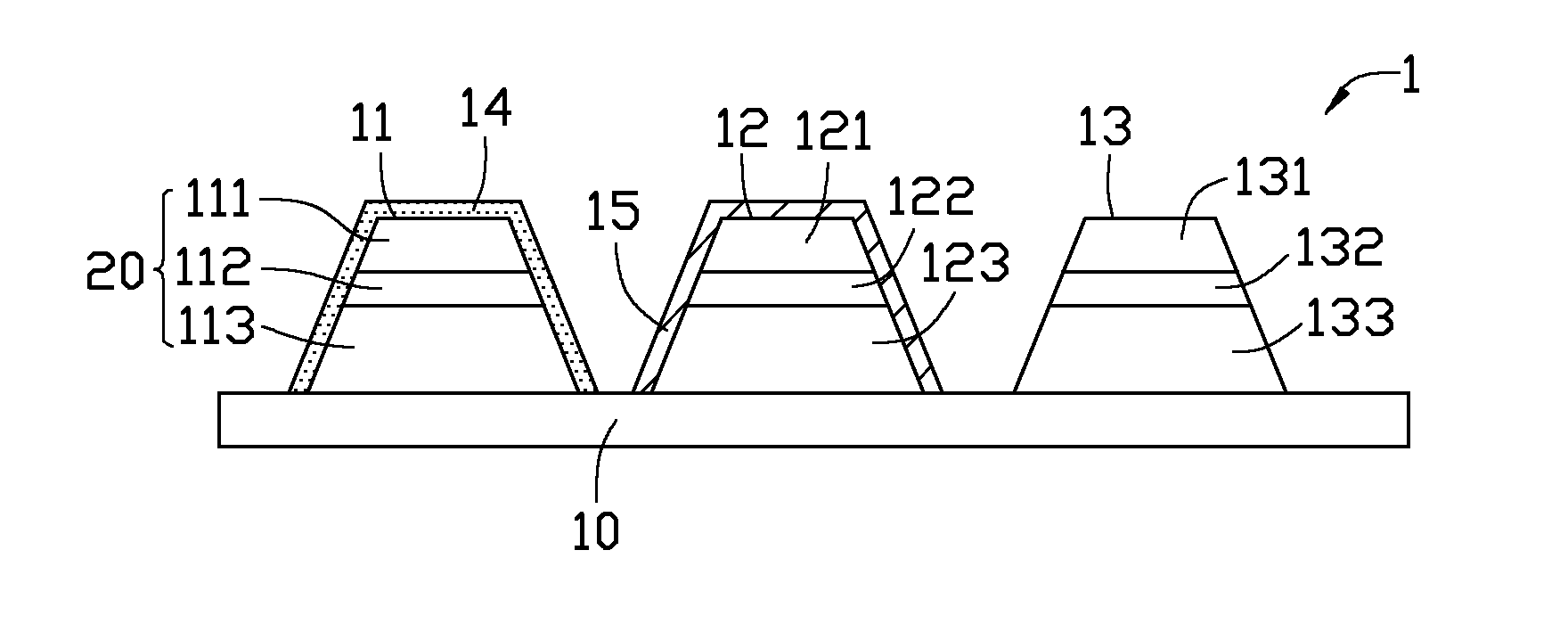
[0012]Referring to FIG. 1, a light emitting diode 1 in accordance with a first embodiment of the disclosure includes a substrate 10, an illumination structure 20, a first fluorescent conversion layer 14, and a second fluorescent conversion layer 15. In the first embodiment, the substrate 10 is a semiconductor substrate of aluminum oxide, silicon carbide, lithium aluminate, lithium gallate, silicon, gallium nitride, zinc oxide, aluminum zinc oxide, gallium arsenide, gallium phosphide, gallium antimonide, indium phosphide, indium arsenide, zinc selenide or metal.

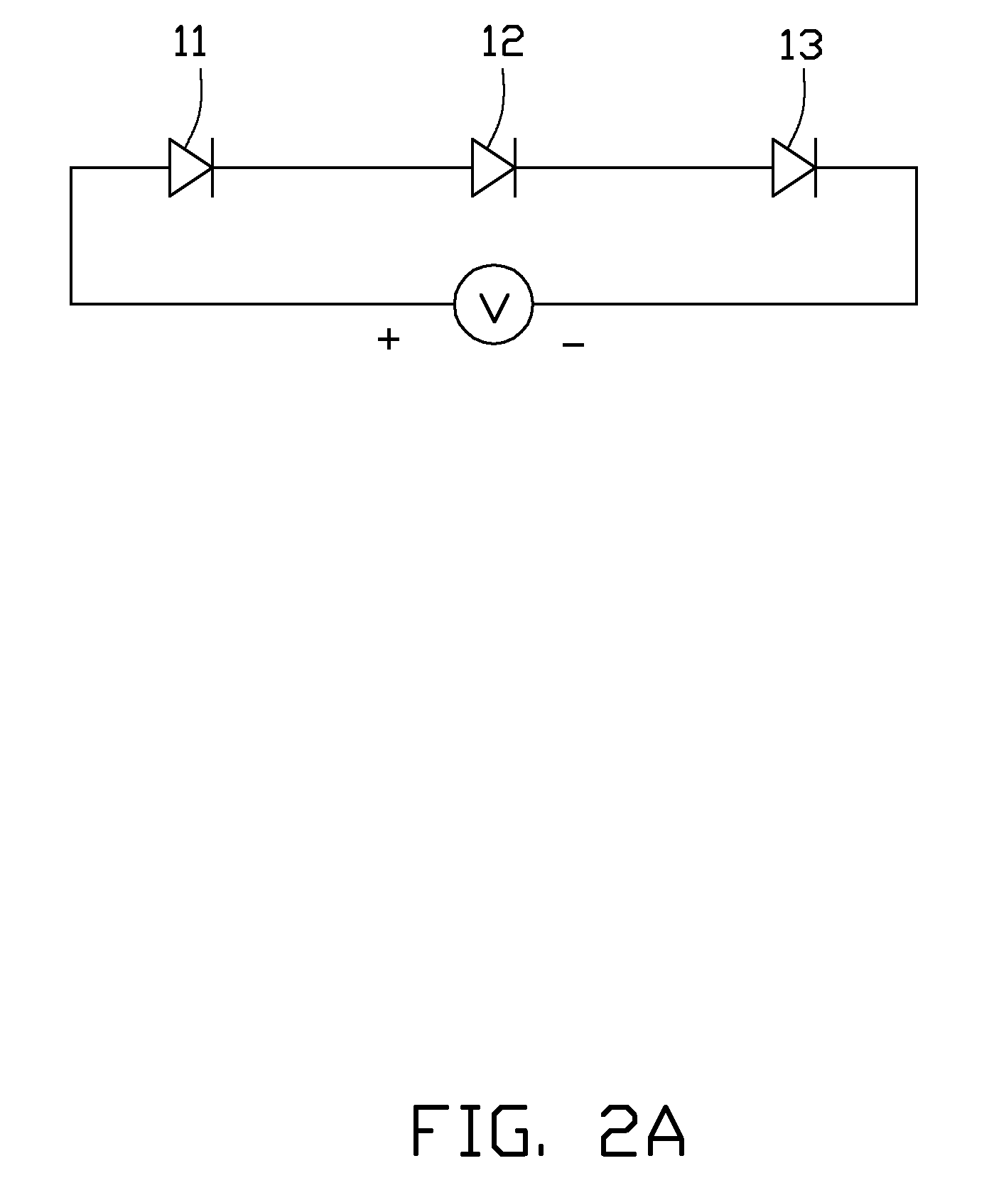
[0013]The illumination structure 20 is disposed on the substrate 10 and includes a first illumination region 11, a second illumination region 12, and a third illumination region 13. In the first embodiment, a space between the first illumination region 11 and the second illumination region 12 or between the second illumination region 12 and the third illumination region 13 is less than 50 μm. The first illumination region 11, ...


PUM


Abstract

A light emitting diode includes a first illumination region, a second illumination region, and the third illumination, wherein a first fluorescent conversion layer and a second fluorescent conversion layer cover the first illumination region and the second illumination region, respectively. The fluorescent conversion layers can convert lights from the illumination regions to other lights with different wavelengths whereby the light emitting diode generates light with multiple wavelengths.

Description

BACKGROUND[0001]1. Technical Field[0002]The disclosure relates generally to light emitting diodes, and more particularly to a light emitting diode with multiple wavelengths.[0003]2. Description of the Related Art[0004]Many illumination products use light emitting diode or laser diodes as a light source, such as environmental lighting or display backlighting, thanks to optimum lifetime, low energy consumption and heat generation, and compact profile. White light is often generated by blue chips packaged with yellow phosphor, or multiple chip packages, such as those combining red, green, and blue chips. U.S. Pat. No. 7,635,870 discloses a multiple chip package like that described.[0005]Although the blue chip with yellow phosphor package can generate white light, the color rendering index (CRI) is insufficient, especially in the red spectrum range, being less than other ranges, such as yellow and green. Additionally, while the multi-chip package has a higher CRI, the different color ch...

Claims


Application Information

Patent Timeline
Patent Type & Authority Applications(United States)
IPC IPC(8): H01L31/12H01L33/50
CPCH01L27/153H01L33/50H01L33/20H01L33/08
Inventor SHEN, CHIA-HUIHUNG, TZU-CHIENTSANG, JIAN-SHIHN
Owner ADVANCED OPTOELECTRONICS TECH
Why Eureka
Try Eureka