Packaging substrate having a passive element embedded therein and method of fabricating the same

a technology of passive elements and packaging substrates, which is applied in the field of packaging substrates, can solve the problems of loss of electricity and electrical functionality, adverse thinning design of electronic devices, and increase the height, and achieve the effect of reducing the overall structural height and shortened signal transmission routes

Active Publication Date: 2012-02-16
UNIMICRON TECH CORP
View PDF26 Cites 20 Cited by
  • Summary
  • Abstract
  • Description
  • Claims
  • Application Information

AI Technical Summary

Benefits of technology

[0027]It can be known from the above that the present invention, through the embedding of the passive element, may have a reduced overall structural height and shortened signal transmission route between the passive element and interlayer circuits, as compared to the prior art. Therefore, more passive elements may be installed, without affecting the layout.

Problems solved by technology

However, a package structure of the prior art, in which the passive element 12 is disposed on the substrate 10, has an increased height, and is adverse in the thinning design for the electronic devices.
Since the passive element 12 is disposed on an external surface of the substrate 10, a signal transmission route between an interlayer circuit and a passive element of the substrate 10 is very long, which results in the loss of electricity and electrical functionality.
Also, the surface of the substrate 10 is occupied by a circuit layout, so an area within which passive elements may be disposed is very limited.
Therefore, how to avoid the drawbacks of the packaging substrate having a passive element of the prior art is becoming one of the popular issues in the art.

Method used


Image

  • Packaging substrate having a passive element embedded therein and method of fabricating the same
  • Packaging substrate having a passive element embedded therein and method of fabricating the same
  • Packaging substrate having a passive element embedded therein and method of fabricating the same

Examples


first embodiment

The First Embodiment

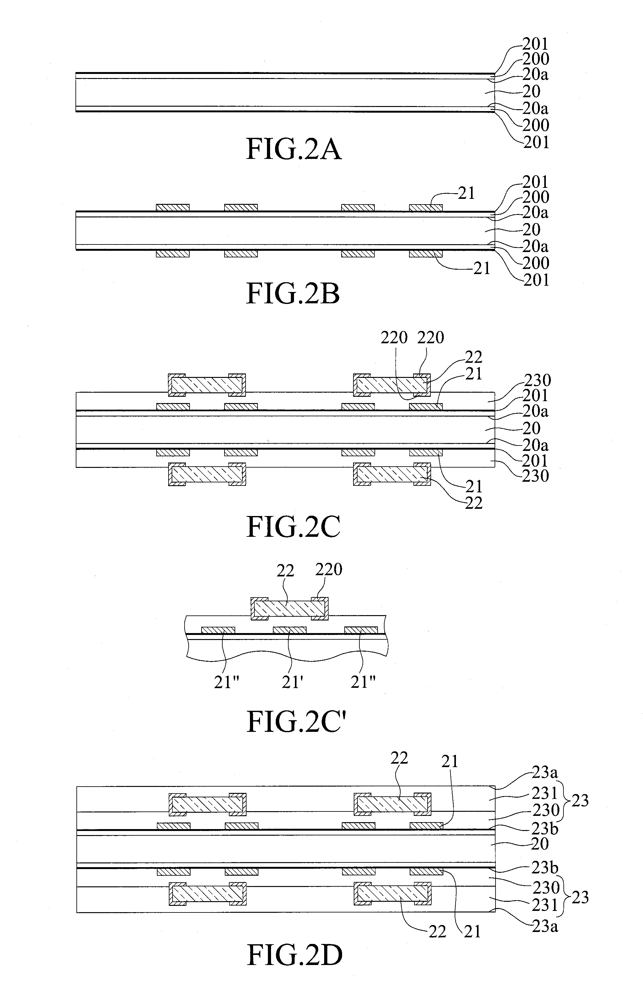
[0035]FIGS. 2A to 2G are cross-sectional diagrams illustrating a method of fabricating a packaging substrate having a passive element embedded therein according to the present invention.

[0036]As shown in FIG. 2A, a carrier board 20 is provided. Two surfaces 20a of the carrier board 20 have release film 200 and metal layers 201 sequentially.

[0037]As shown in FIG. 2B, a positioning pad 21 is formed on the metal layer 201.

[0038]As shown in FIG. 2C, the metal layers 201 on the two surfaces 20a of the carrier board 20 are encapsulated by a first thermalplastic dielectric layer 230; a passive element 22 is provided that has a plurality of electrode pads 220 disposed on upper and lower surfaces thereof; and the passive element 22 is disposed on the first thermalplastic dielectric layer 230, with the positioning pad 21 as a positioning site, wherein the electrode pads 220 disposed on the lower surface of the passive element 22 correspond in position to the positioning pa...

second embodiment

The Second Embodiment

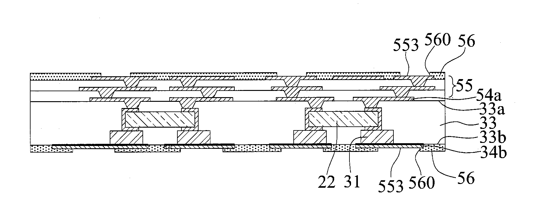
[0046]Please refer to FIGS. 3A to 3F. The second embodiment differs from the first embodiment in that in the second embodiment, the solder bumps are replaced with positioning pads, and the dielectric layer unit and the second circuit layer are fabricated by different processes.

[0047]As shown in FIG. 3A, a carrier board shown in FIG. 2A is provided, and solder bumps 31 are formed on the metal layer 201.

[0048]As shown in FIG. 3B, a passive element 22 shown in FIG. 2C is provided, and electrode pads 220 disposed on a lower surface of the passive element 22 are disposed on the solder bumps 31.

[0049]As shown in FIG. 3C, two dielectric layer units 33, each of which has top and bottom surfaces 33a and 33b, are formed on the metal layers 201; the passive element 22 is embedded in the dielectric layer unit 33; and the solder bumps 31 are embedded in the bottom surface 33b of the dielectric layer unit 33.

[0050]As shown in FIG. 3D, the carrier board 20 and the release film...

third embodiment

The Third Embodiment

[0054]Please refer to FIGS. 4A to 4D. The third embodiment differs from the first embodiment in the processes of fabricating the first circuit layer and the circuit built-up structure.

[0055]As shown in FIG. 4A, subsequent to the fabrication process shown in FIG. 2D, in which the dielectric layer unit 23 is formed by the heating and compressing processes, a first circuit layer 44a is formed on the top surface 23a of the dielectric layer unit 23, and the first circuit layer 44a has first conductive vias 440a electrically connected to the electrode pads 220 disposed on the upper surface of the passive element 22; and a circuit built-up structure 45 is then formed on the top surface 23a of the dielectric layer unit 23 and the first circuit layer 44a. The circuit built-up structure 45 comprises at least a dielectric layer 450, a circuit layer 451 disposed on the dielectric layer 450, and conductive vias 452 disposed in the dielectric layer 450 and electrically connect...


PUM

PropertyMeasurementUnit
conductiveaaaaaaaaaa
resistancesaaaaaaaaaa
voltagesaaaaaaaaaa

Abstract

A packaging substrate includes: a dielectric layer unit having top and bottom surfaces; a positioning pad embedded in the bottom surface of the dielectric layer unit; at least a passive element having a plurality of electrode pads disposed on upper and lower surfaces thereof, the passive element being embedded in the dielectric layer unit and corresponding to the positioning pad; a first circuit layer disposed on the top surface of the dielectric layer unit, the first circuit layer having first conductive vias electrically connected to the electrode pads disposed on the upper surface of the passive element; and a second circuit layer disposed on the bottom surface of the dielectric layer unit, the second circuit layer having second conductive vias electrically connected to the electrode pads disposed on the lower surface of the passive element. Through the embedding of the passive element, the overall structure may have a reduced height.

Description

BACKGROUND OF THE INVENTION[0001]1. Field of the Invention[0002]This invention relates to packaging substrates and methods of fabricating the same, and, more particularly, to a packaging substrate having a passive element and a method of fabricating the same.[0003]2. Description of Related Art[0004]With the rapid development of semiconductor package technology, passive elements are in increasing demands. Passive elements do not affect the basic characteristics of signal, but only allow the signals to pass therethrough. Passive elements include capacitors, resistors and inductors. Compared to active elements, the passive elements have their resistances unchanged even when voltages or currents change, because the passive elements do not participate in electron exercises.[0005]Any product that is driven by electricity needs passive elements that provide electrical loop controlling functions. Such applications include 3C and other industrial fields. Please refer to FIG. 1, which is a cr...

Claims


Application Information

Patent Timeline
Patent Type & Authority Applications(United States)
IPC IPC(8): H05K7/20H05K1/16B23K1/19B32B38/10B23K1/00
CPCH01L23/49822H01L23/50H05K1/187H05K3/0097H05K3/4602H05K2201/0129H05K2201/10636H05K2203/1469H05K2203/1536H01L2924/0002H01L2924/00H05K3/4038H05K3/4644H05K3/4679H05K1/113H05K1/183H05K1/185Y10T29/4913Y10T29/49146Y02P70/611Y02P70/50
Inventor HSU, SHIH- PINGZENG, ZHAO-CHONG
Owner UNIMICRON TECH CORP
Why Eureka
Try Eureka