Plasma processing apparatus and plasma control method

a processing apparatus and plasma technology, applied in the field of plasma processing apparatus, can solve the problems of difficult control of plasma density in the processing chamber to a desired state, inability to perform a uniform plasma process on the substrate, and non-uniform plasma density within the processing chamber

Active Publication Date: 2012-02-16
TOKYO ELECTRON LTD
View PDF7 Cites 12 Cited by
  • Summary
  • Abstract
  • Description
  • Claims
  • Application Information

AI Technical Summary

Benefits of technology

[0029]In accordance with the present disclosure, the plasma distribution within the processing chamber can be controlled to be a desired state. Thus, it may be possible to uniformize the plasma density within the processing chamber, and also possible to perform a uniform plasma process on the substrate.

Problems solved by technology

Accordingly, a plasma density within the chamber may become non-uniform and there is a problem that it may not be possible to perform a uniform plasma process on the substrate.
Thus, it may be still difficult to control the plasma density in the processing chamber to a desired state.

Method used


Image

  • Plasma processing apparatus and plasma control method
  • Plasma processing apparatus and plasma control method
  • Plasma processing apparatus and plasma control method

Examples


first embodiment

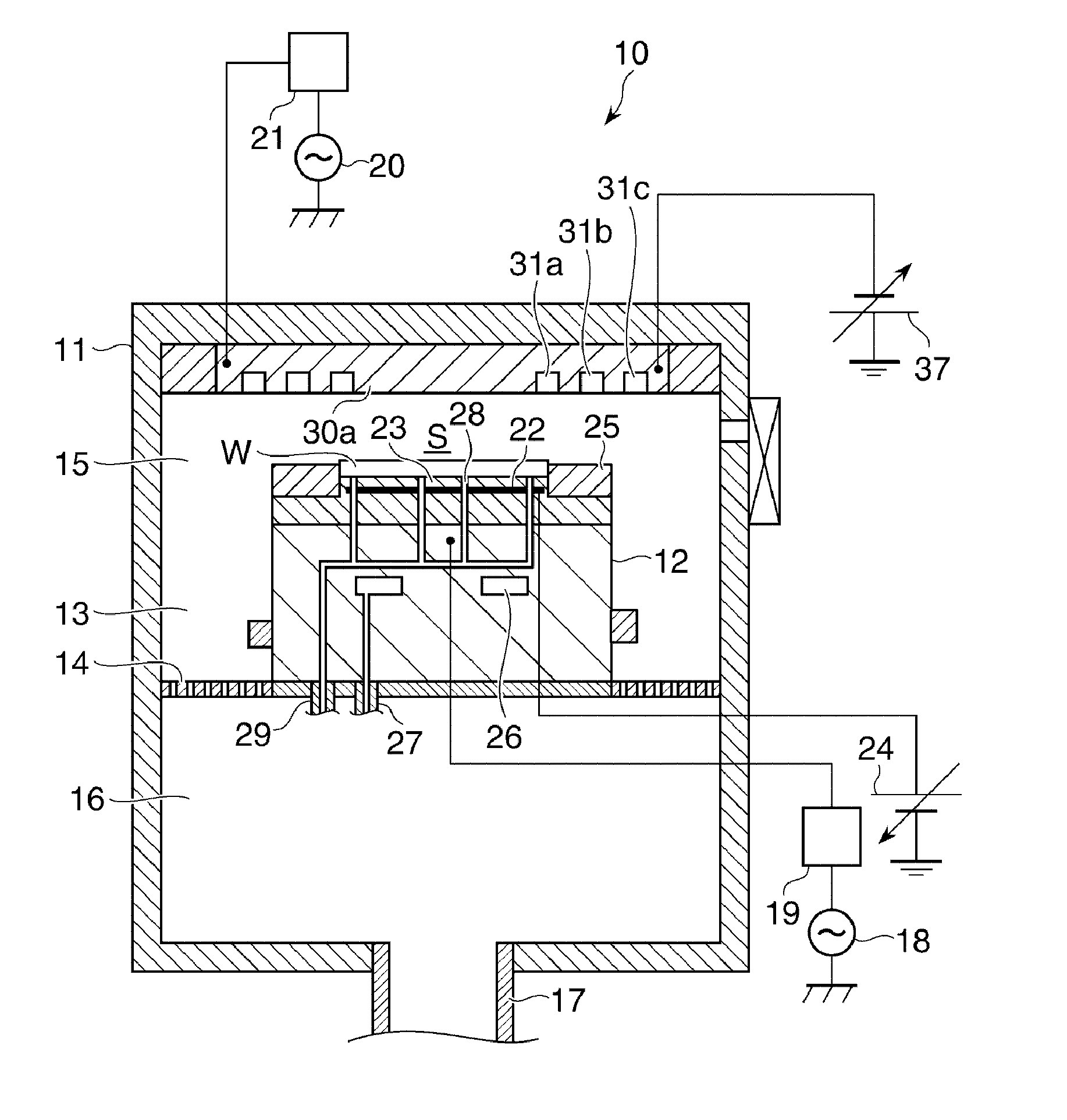
[0040]FIG. 1 is a cross sectional view schematically illustrating a configuration of a plasma processing apparatus in accordance with the present disclosure. This plasma processing apparatus performs a plasma process such as etching process or film forming process on, e.g., a semiconductor wafer (hereinafter, simply referred to as a “wafer”).

[0041]As depicted in FIG. 1, a plasma processing apparatus may include a processing chamber 11 that accommodates therein a substrate (hereinafter, simply referred to as a “wafer”) W. A cylindrical susceptor 12 for mounting thereon the wafer W is provided within the chamber 11. A side exhaust path 13 is formed between an inner sidewall of the chamber 11 and a side surface of the susceptor 12. An exhaust plate 14 is provided on the way of the side exhaust path 13.

[0042]The exhaust plate 14 is a plate-shaped member having a multiple number of through holes and serves as a partition plate that partitions the inside of the chamber 11 into an upper re...

second embodiment

[0088]Now, a plasma processing apparatus in accordance with the present disclosure will be explained.

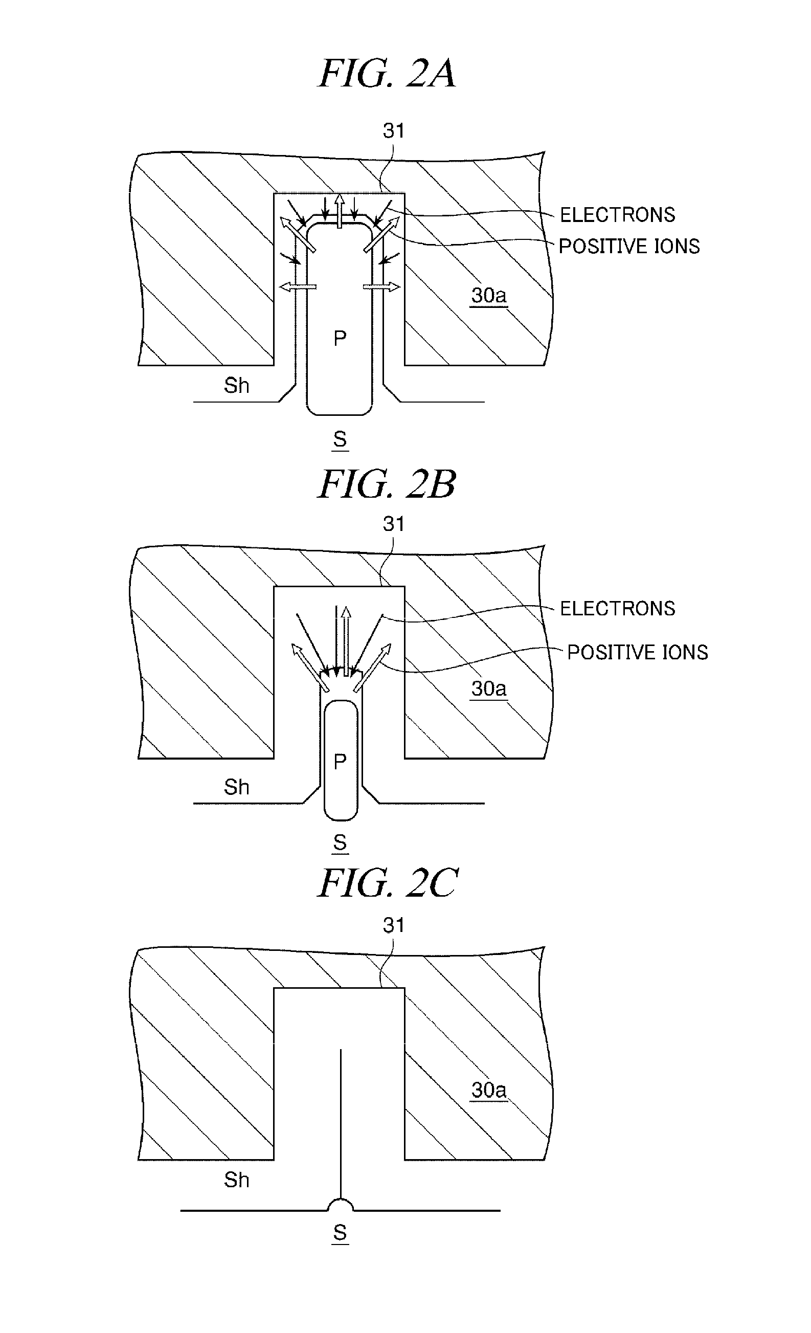
[0089]FIG. 5 is a cross sectional view schematically illustrating a configuration of the plasma processing apparatus in accordance with the second embodiment. A plasma processing apparatus 50 in FIG. 5 is different from the plasma processing apparatus 10 of FIG. 1 in that there is provided an upper electrode plate 30b having hollow cathodes 31d to 31f with different depths, instead of the upper electrode plate 30a having the hollow cathodes 31a to 31c with the same depths. The depths of the hollow cathodes 31d to 31f increase as the hollow cathode is distanced away from the center of the upper electrode plate 30b.

[0090]In accordance with the second embodiment, by forming the hollow cathodes 31d to 31f at the peripheral portion of the upper electrode plate 30b corresponding to the peripheral region of the processing space S, a plasma density in the peripheral region of the processing...

third embodiment

[0099]Now, a plasma processing apparatus in accordance with the present disclosure will be explained.

[0100]FIG. 7 is a cross sectional view schematically illustrating a configuration of major parts of the plasma processing apparatus in accordance with the third embodiment.

[0101]In a plasma processing apparatus 70 illustrated in FIG. 7, inner wall members 71a and 71b made of a conductor such as Si are provided at left and right sidewall surfaces of the chamber 11. Hollow cathodes 72 are formed at upper and lower portions of the inner wall members 71a and 71b.

[0102]Further, the inner wall members 71a and 71b having the hollow cathodes 72 are electrically connected with DC power supplies 37a and 37b, respectively.

[0103]In accordance with the third embodiment, plasma density in upper and lower portions of the peripheral region of the processing space S can be increased, so that an overall plasma density within the processing space S can be uniformized.

[0104]That is, if plasma is genera...


PUM

PropertyMeasurementUnit
self bias voltageaaaaaaaaaa
frequencyaaaaaaaaaa
frequency poweraaaaaaaaaa

Abstract

There is provided a plasma processing apparatus capable of performing a uniform plasma process on a substrate by controlling a plasma distribution within a chamber to a desired state and uniformizing a plasma density within the chamber. The plasma processing apparatus includes an evacuable chamber 11 for performing a plasma process on a wafer W; a susceptor 12 for mounting the wafer W within the chamber 11; an upper electrode plate 30a facing the susceptor 12 with a processing space S; a high frequency power supply 20 for applying a high frequency power to one of the susceptor 12 and the upper electrode plate 30a to generate plasma within the processing space S; and an inner wall member facing the processing space S. Hollow cathodes 31a to 31c are formed at the upper electrode plate 30a connected with a DC power supply 37 for adjusting a sheath voltage.

Description

CROSS-REFERENCE TO RELATED APPLICATION[0001]This application claims the benefit of Japanese Patent Application No. 2010-180237 filed on Aug. 11, 2010 and U.S. Provisional Application Ser. No. 61 / 377,497 filed on Aug. 27, 2010, the entire disclosures of which are incorporated herein by reference.FIELD OF THE INVENTION[0002]The present disclosure relates to a plasma processing apparatus capable of controlling a plasma distribution within a processing chamber and a plasma control method.BACKGROUND OF THE INVENTION[0003]In a manufacturing process of a semiconductor device or a flat panel display (FPD) such as a liquid crystal display (LCD), there is known a plasma processing apparatus for performing a plasma process on various kinds of substrates such as a glass substrate. The plasma processing apparatus may be classified into a capacitively coupled plasma processing apparatus and an inductively coupled plasma processing apparatus according to a method for generating plasma.[0004]Known ...

Claims


Application Information

Patent Timeline
Patent Type & Authority Applications(United States)
IPC IPC(8): C23F1/00C23C16/50C23C16/458C23F1/08H05H1/24
CPCH01J37/32091H01J37/32697H01J37/32596
Inventor KOSHIMIZU, CHISHIODENPOH, KAZUKI
Owner TOKYO ELECTRON LTD
Why Eureka
Try Eureka