

Method and apparatus for measuring electron density of plasma and plasma processing apparatus
a plasma processing and electron density technology, applied in the direction of electrical excitation analysis, semiconductor/solid-state device testing/measurement, instruments, etc., can solve the problems of difficult observation of net power absorption, easy deviation of measured value, and easy error of measured value, etc., to achieve stable and high-speed probe scanning
- Summary
- Abstract
- Description
- Claims
- Application Information
AI Technical Summary
Benefits of technology
Problems solved by technology
Method used
Image

Examples
embodiment 1
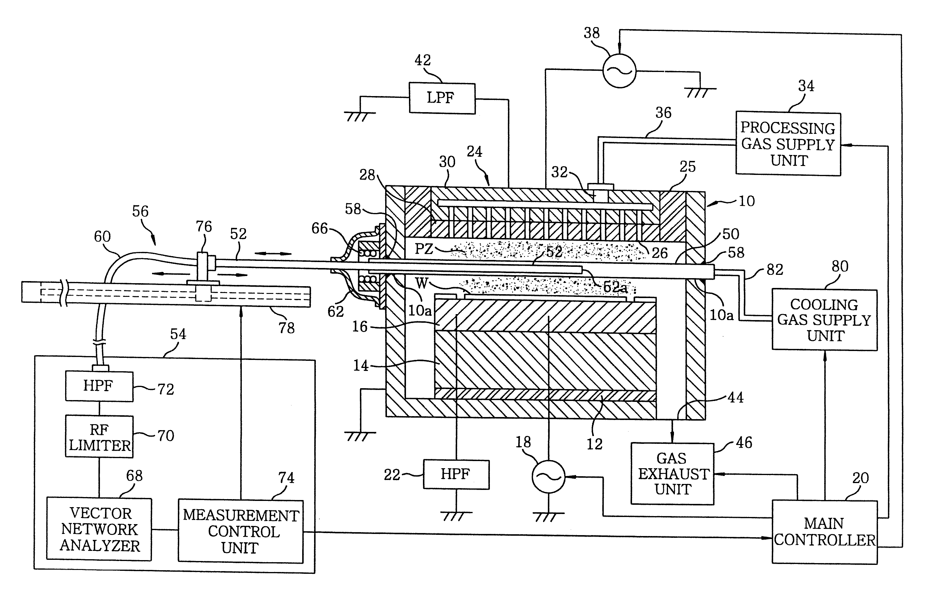
[0067] With reference to FIGS. 1 to 18, a first embodiment of the present invention is described. FIGS. 1 and 2 show a configuration of a plasma processing apparatus, to which a method and an apparatus for measuring electron density of plasma are applied, in accordance with a first embodiment of the present invention. This plasma processing apparatus is a capacitively coupled parallel flat plate type plasma processing apparatus.
[0068] A chamber 10 of the plasma processing apparatus is made of, for example, aluminum, and is composed of a processing chamber that is cylindrically shaped and can be sealed. A support 14 made of, e.g., aluminum is placed on the bottom of the chamber 10 with an insulating plate 12 being interposed therebetween, and a susceptor 16 made of, e.g., aluminum is seated on the support 14. The susceptor 16 constitutes a lower electrode, and a substrate to be processed, such as a semiconductor wafer W, is mounted thereon.
[0069] A high frequency power supply 18 fo...
embodiment 3
[0202] Next, with reference to FIGS. 32 to 48, an embodiment of the plasma light emission measuring method of the present invention is described. FIG. 32 shows a configuration of a plasma processing apparatus to which plasma light emission measuring method and apparatus in accordance with a third embodiment of the present invention are applied. In these drawings, elements having same configurations and functions as those in the plasma processing apparatus and plasma monitoring apparatus of FIG. 1 are assigned same reference numerals, and detailed descriptions thereof are omitted.
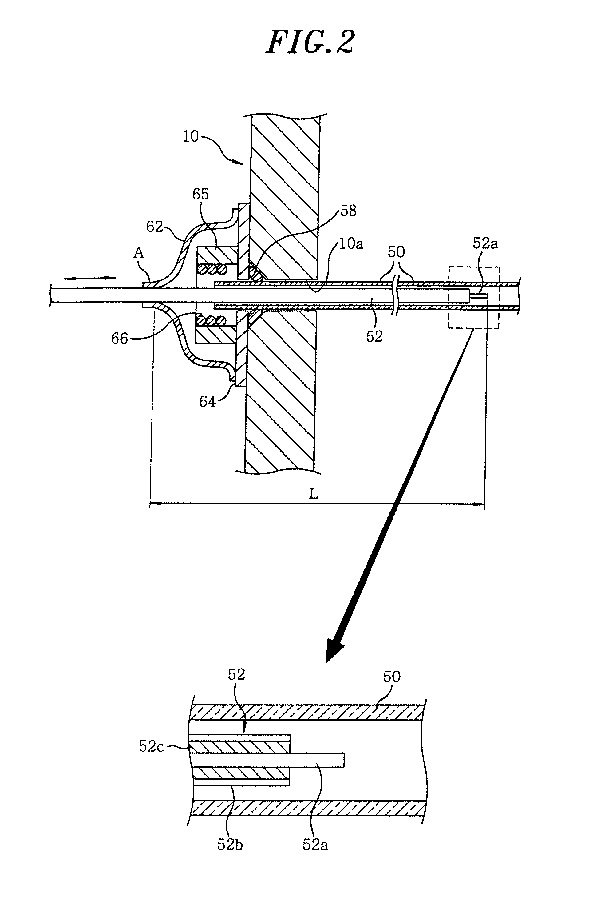
[0203] The plasma light emission measuring apparatus of the present embodiment includes a cylindrical transparent insulating pipe 50 fixedly attached to a chamber 10, a rod-shaped optical transmission probe 130 provided with a light receiving surface 130a at a front end thereof and inserted into a quartz pipe 50 through one end of the quartz pipe 50 (left-hand side of FIG. 1) to slide therethrough, a measur...
PUM
| Property | Measurement | Unit |
|---|---|---|
| frequency | aaaaa | aaaaa |
| frequency | aaaaa | aaaaa |
| frequency | aaaaa | aaaaa |
Abstract
Description
Claims
Application Information