Disturb-resistant non-volatile memory device and method

a non-volatile memory and resistive technology, applied in the direction of bulk negative resistance effect devices, semiconductor devices, electrical equipment, etc., can solve the problems of increasing power dissipation, non-scaling of sub-threshold slopes, and reducing device performan

Active Publication Date: 2012-02-23
INNOSTAR SEMICON SHANGHAI CO LTD
View PDF5 Cites 56 Cited by
  • Summary
  • Abstract
  • Description
  • Claims
  • Application Information

AI Technical Summary

Problems solved by technology

However, as field effect transistors (FET) approach sizes less than 100 nm, problems such as short channel effect can degrade device performance.
Moreover, such sub 100 nm device size can lead to sub-threshold slope non-scaling and also increases power dissipation.
These devices often require new materials and device structures to couple with silicon-based devices to form a memory cell, which lack one or more key attributes.
For example, Fe-RAM and MRAM devices have fast switching characteristics and good programming endurance, but their fabrication is not CMOS compatible and size is usually large.
Power dissipation during switching for a PCRAM device is usually large.
Organic RAM or ORAM is incompatible with large volume silicon-based fabrication and device reliability is usually poor.

Method used


Image

  • Disturb-resistant non-volatile memory device and method
  • Disturb-resistant non-volatile memory device and method
  • Disturb-resistant non-volatile memory device and method

Examples


Embodiment Construction

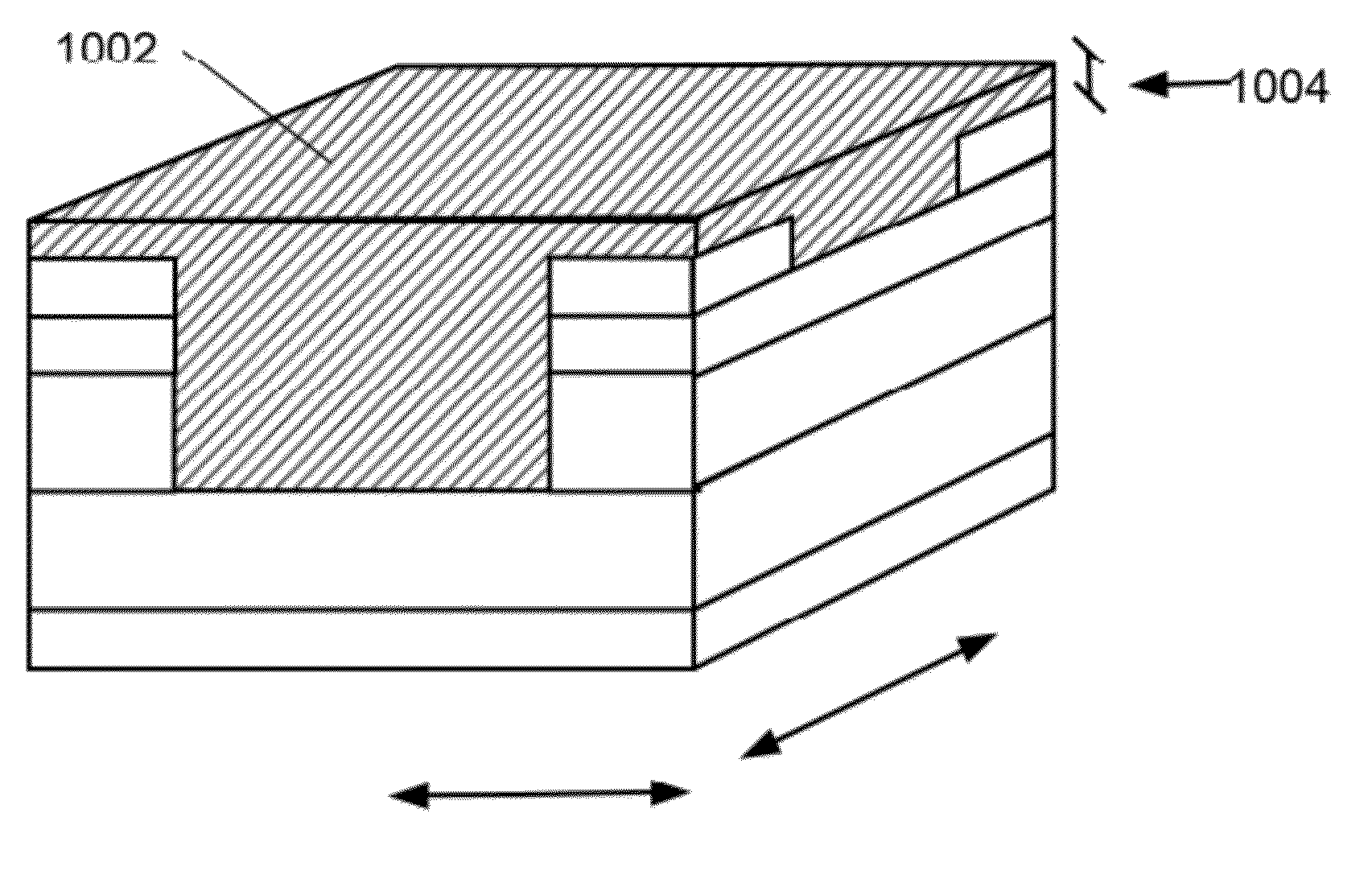
[0015]The present invention is generally related to switching devices. More particularly, embodiments according to the present invention provide a method and a structure to form an array of switching devices. The present invention has be applied to forming a disturb resistant non-volatile memory device using an amorphous silicon switching material. But it should be recognized that embodiments of the present invention can be applied to other devices.

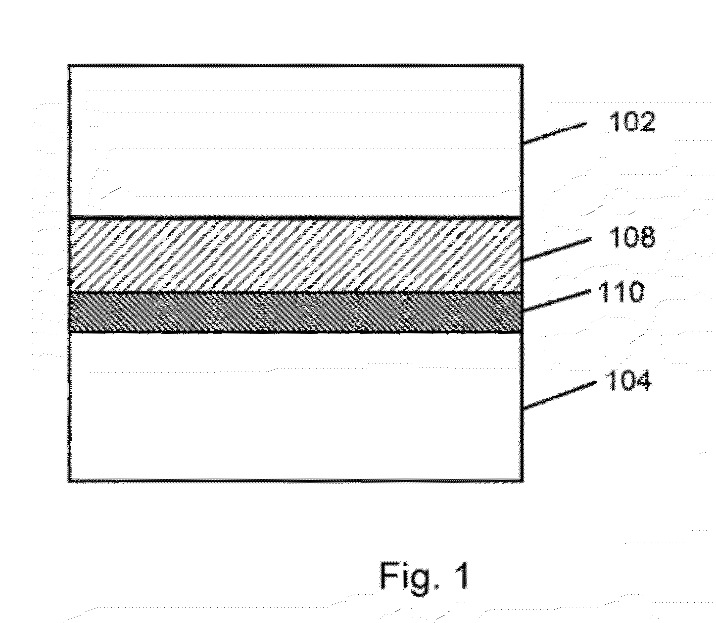
[0016]FIG. 1 is a simplified diagram illustrating a cross section of a resistive switching device 100. The resistive switching device includes a top wiring structure 102, a bottom wiring structure 104 and a switching element 108 disposed between the top wiring structure and the bottom wiring structure. The top electrode and the bottom electrode are arranged orthogonal to each other in a crossbar to form a highly interconnected structure. In this implementation, the top wiring structure and the bottom wiring structure can have a portion in...


PUM

PropertyMeasurementUnit
sizesaaaaaaaaaa
sizeaaaaaaaaaa
angleaaaaaaaaaa

Abstract

A method of forming a disturb-resistant non volatile memory device. The method includes providing a semiconductor substrate having a surface region and forming a first dielectric material overlying the surface region. A first wiring material overlies the first dielectric material, a doped polysilicon material overlies the first wiring material, and an amorphous silicon switching material overlies the said polysilicon material. The switching material is subjected to a first patterning and etching process to separating a first strip of switching material from a second strip of switching spatially oriented in a first direction. The first strip of switching material, the second strip of switching material, the contact material, and the first wiring material are subjected to a second patterning and etching process to form at least a first switching element from the first strip of switching material and at least a second switching element from the second strip of switching material, and a first wiring structure comprising at least the first wiring material and the contact material. The first wiring structure being is in a second direction at an angle to the first direction.

Description

CROSS REFERENCE TO RELATED APPLICATIONS[0001]Not ApplicableBACKGROUND[0002]The present invention is generally related to resistive switching devices. More particularly, embodiments according to the present invention provide a method and a structure for forming a vertical resistive switching device. The present invention can be applied to non-volatile memory devices but it should be recognized that the present invention can have a much broader range of applicability[0003]The success of semiconductor devices has been mainly driven by an intensive transistor down-scaling process. However, as field effect transistors (FET) approach sizes less than 100 nm, problems such as short channel effect can degrade device performance. Moreover, such sub 100 nm device size can lead to sub-threshold slope non-scaling and also increases power dissipation. It is generally believed that transistor-based memories such as those commonly known as Flash may approach an end to scaling within a decade. Flash...

Claims


Application Information

Patent Timeline
Patent Type & Authority Applications(United States)
IPC IPC(8): H01L29/04H01L47/00
CPCH01L45/085H01L45/148H01L45/1675H01L27/2481H01L45/1608H01L27/2463H01L45/1253H01L45/14H01L27/2436H10N70/245H10N70/884H10N70/063H10B63/80H10B63/30H10B63/84H10N70/021H10N70/841H10N70/881
Inventor HERNER, SCOTT BRADNAZARIAN, HAGOP
Owner INNOSTAR SEMICON SHANGHAI CO LTD
Why Eureka
Try Eureka