Organic electroluminescence display device and manufacturing method therefor
- Summary
- Abstract
- Description
- Claims
- Application Information
AI Technical Summary
Benefits of technology
Problems solved by technology
Method used
Image

Examples
example 1
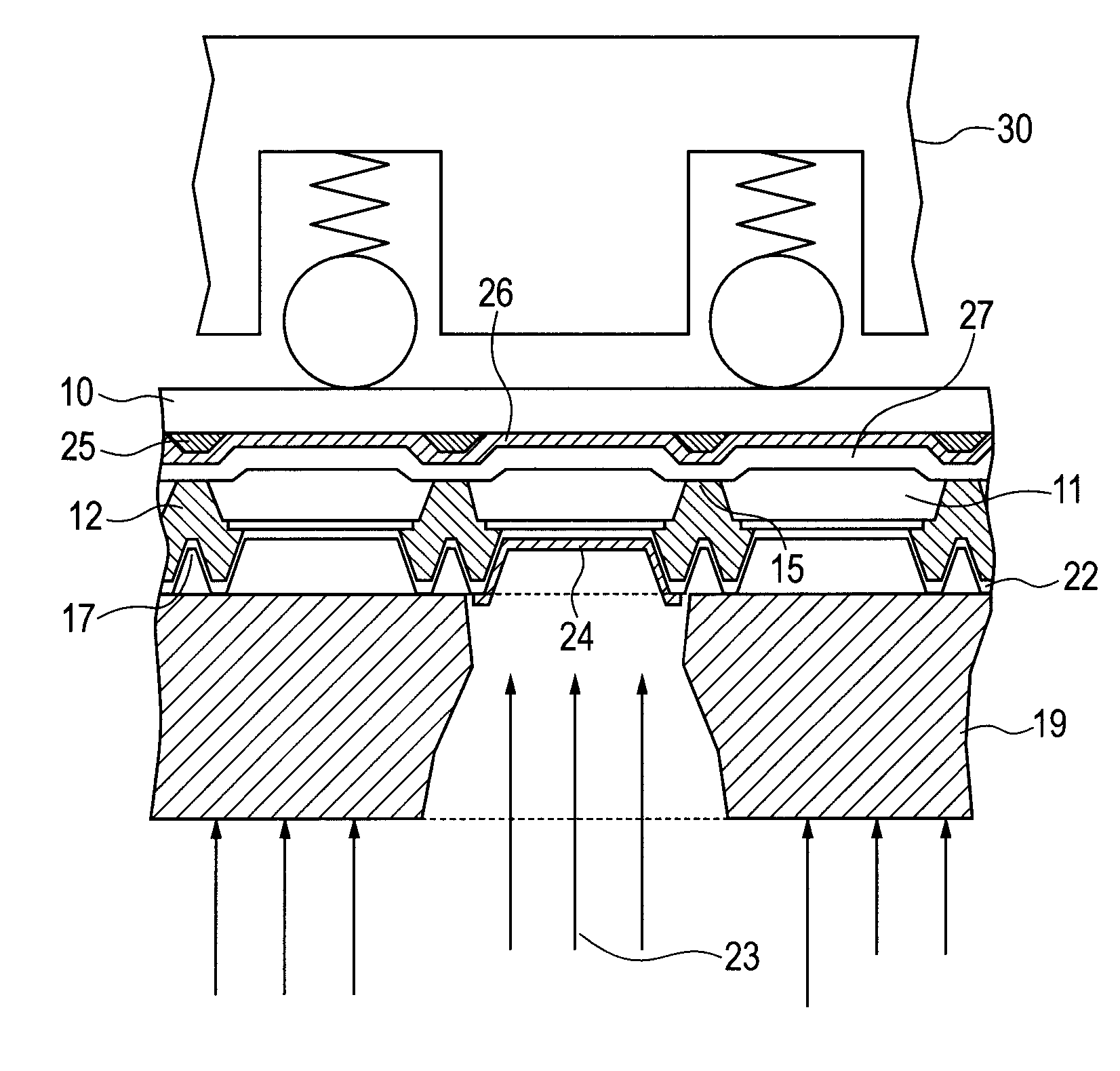
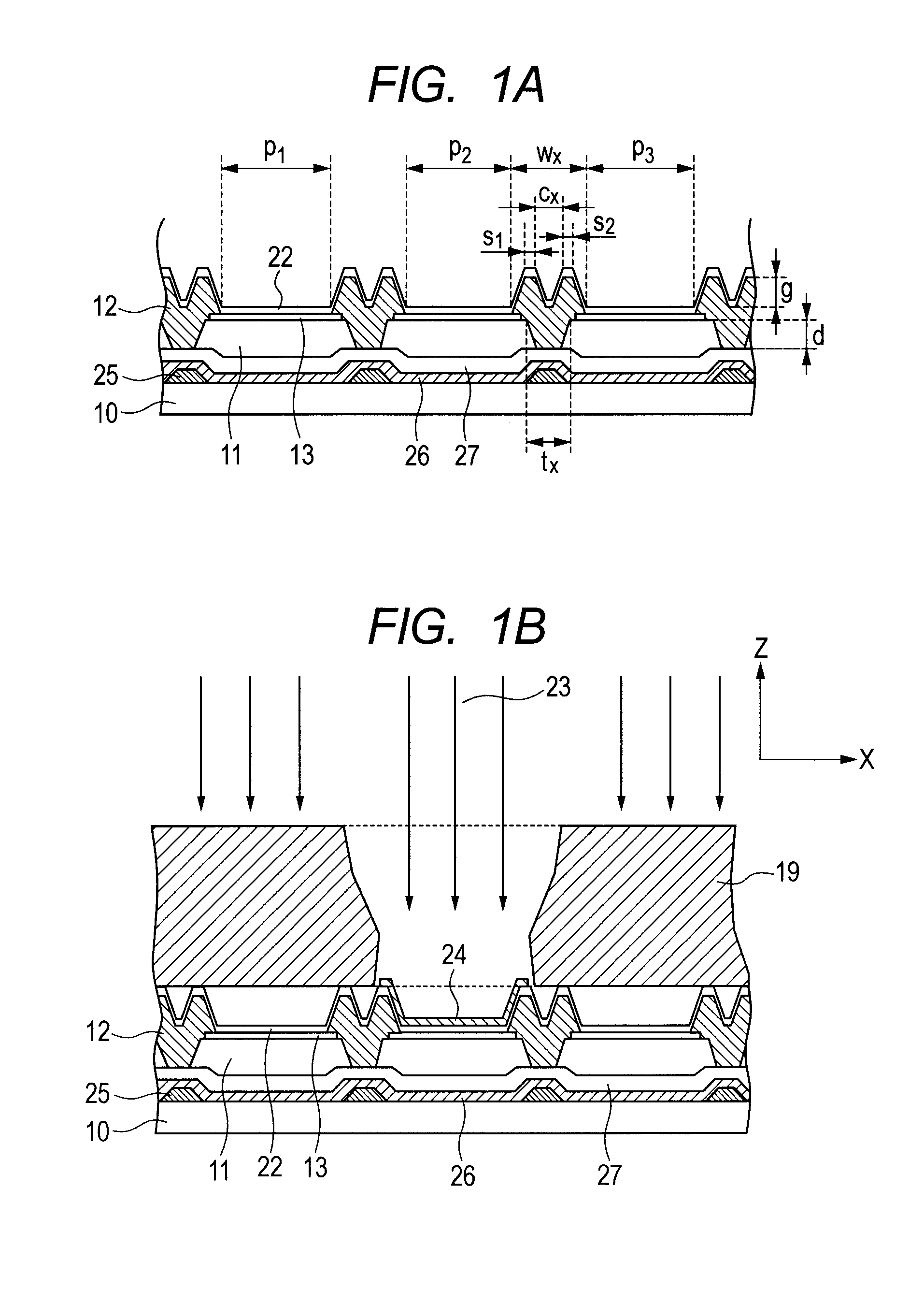
[0062]With reference to FIGS. 1A and 1B, 2, and 3A to 3E, a manufacturing method for the organic EL display device according to Example 1 is described. FIG. 1A schematically illustrates a cross sectional structure of one pixel region, and illustrates a state where the hole transport layer 22 is formed to have the same thickness in all pixels. When multiple pixels having the cross sectional structure illustrated in FIG. 1A are arranged in matrix, a display region of the organic EL display device is constituted. In addition, three sub-pixels including p1, p2 and p3 are arranged in parallel in one pixel region. Note that, the organic EL display device described here has a pixel pitch of 191 μm and a sub-pixel size of 64 μm×191 μm.
[0063]As illustrated in FIGS. 1A and 3A, transistors are formed correspondingly to individual sub-pixels on the substrate 10. Note that, in FIGS. 1A and 1B, only gate lines 25 of the transistors, the gate insulating layer 26, and a passivation layer (insulatin...
example 2
[0076]With reference to FIG. 7, a manufacturing method for an organic EL display device according to Example 2 is described. FIG. 7 illustrates a process of forming the emission layer in the sub-pixel. Note that, the substrate described in this example has a size of 60 mm×460 mm×0.5 mmt, and 5×5 panel regions are disposed. In each panel region, the structure of the transistor, the first insulating layer 11, the first electrode 13, and the second insulating layer 12 formed on the substrate 10 is the same as in Example 1.
[0077]As illustrated in FIG. 7, when the vapor deposition of the emission layer is performed, the vapor deposition mask 19 having the opening that exposes the first electrode 13 in the sub-pixel p2 is positioned so as to contact with the hole transport layer 22 deposited on the surface of the second insulating layer 12. Particularly in this example, after positioning the substrate with respect to the vapor deposition mask 19, the substrate is pressed to the vapor depo...
example 3
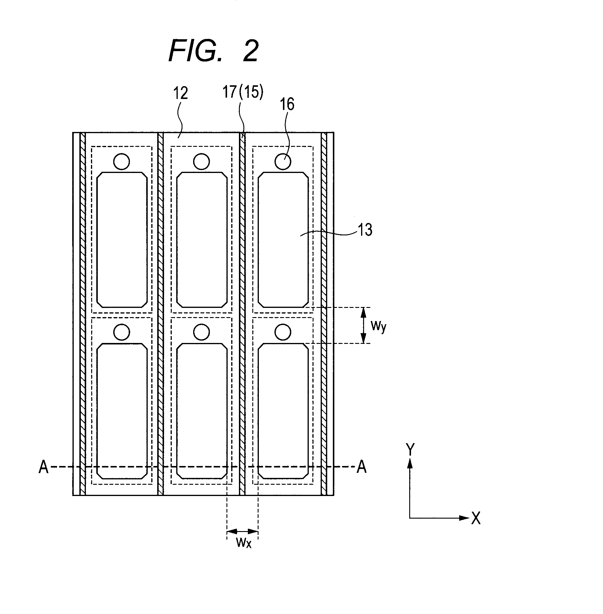
[0080]With reference to FIG. 8B, a manufacturing method for an organic EL display device according to Example 3 is described. FIG. 8B schematically illustrates a plane structure of a 3×2 sub-pixel region, and multiple sub-pixel regions are disposed in matrix so that the display region of the organic EL display device is constituted.
[0081]The second insulating layer 12 illustrated in FIG. 8B is formed so as to have the recesses 17 reflecting the openings 15 by forming the grating-like openings 15 in the peripheries of the first electrodes 13 in the first insulating layer 11. The grating-like opening 15 is formed to communicate to the contact hole 16 that can electrically connect the first electrode 13 to the drain electrode of the transistor.
[0082]The opening 15 having a depth of 2 μm and a width of 20 μm is formed in the first insulating layer 11 between the first electrodes neighboring in an X direction in FIG. 8B, and the second insulating layer 12 is formed to surround the first ...
PUM
 Abstract
Description
Claims
Application Information
PatSnap Eureka turns technology decisions into work you can execute. Powered by our Innovation Knowledge Graph, it runs expert workflows across engineering, life sciences, materials and intellectual property. Get your review-ready output in minutes.


