Semiconductor device

a semiconductor device and semiconductor technology, applied in semiconductor devices, instruments, electrical equipment, etc., can solve the problems of increasing the area of the memory cell, increasing the size of the memory-embedded semiconductor device in which the sram is embedded, and severely restricting the flexibility of designing a wiring pattern in the uppermost metal layer

Active Publication Date: 2012-02-23
SEMICON COMPONENTS IND LLC
View PDF5 Cites 5 Cited by
  • Summary
  • Abstract
  • Description
  • Claims
  • Application Information

AI Technical Summary

Problems solved by technology

The restrictions would increase the area of the memory cell and increase the size of the memory-embedded semiconductor device in which the SRAM is formed.
Also, there are cases in which flexibility in designing a wiring pattern in an uppermost metal layer is severely restricted, depending on design rules applied to metal layers used in multi-layer wirings.
For example, when the design rules impose a restriction that a thick external connection electrode such as a bonding pad is to be formed of the uppermost metal layer, fine wiring pattern is not available with the uppermost metal layer.

Method used


Image

  • Semiconductor device
  • Semiconductor device
  • Semiconductor device

Examples


Embodiment Construction

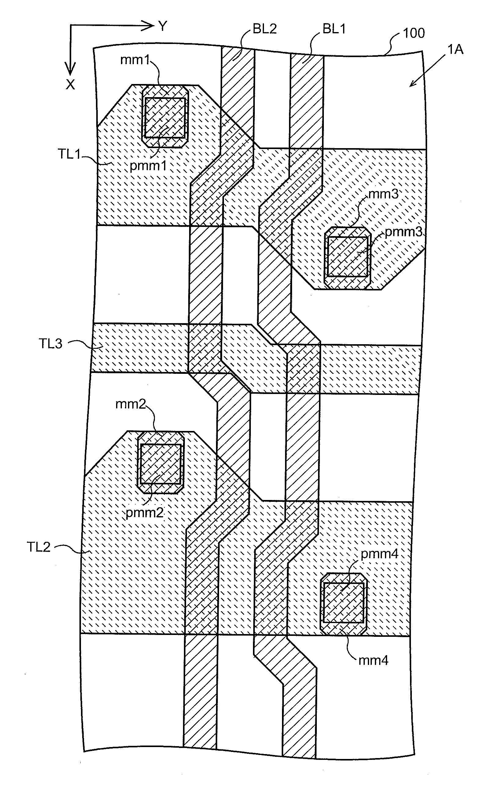
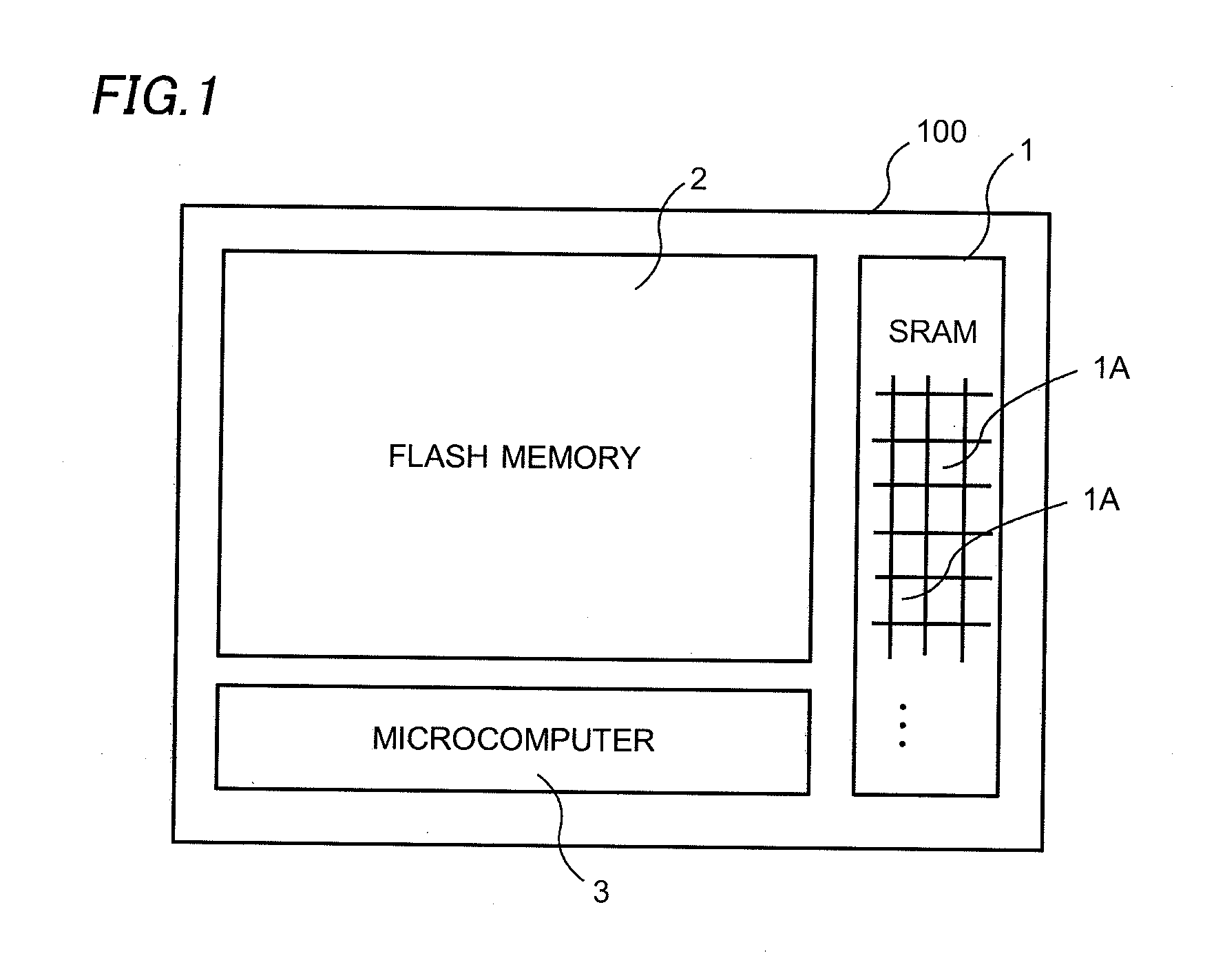
[0020]A semiconductor device according to an embodiment of this invention will be described referring to the drawings. FIG. 1 is a plan view showing an outline structure of the semiconductor device. A static type semiconductor memory (hereafter referred to as an SRAM 1) made of a regular array of a plurality of memory cells 1A is disposed on a semiconductor substrate 100, as shown in FIG. 1. Also, a flash memory 2 and a microcomputer 3 that controls the SRAM 1 and the flash memory 2 are disposed on the semiconductor substrate 100. They form a memory-embedded semiconductor device, which is a single semiconductor chip.

[0021]The flash memory 2 serves as a large storage capacity (4 M bytes, for example) memory compared with the SRAM 1 that serves as a small storage capacity (256 K bytes, for example) buffer memory. In this case, a ratio of an area occupied by the flash memory 2 to a total area of the semiconductor substrate 100 (about 90%, for example) is significantly larger than a rat...


PUM


Abstract

In a memory cell including CMOS inverters, an increase in an area of the memory cell caused by restrictions on a gate wiring due to a leakage current and restrictions due to design rules is suppressed. A first wiring and a second wiring are laid out as a first metal layer in the memory cell that includes a first inverter and a second inverter. The first wiring is connected with two drains in the first inverter and a second gate wiring in the second inverter. The second wiring is connected with two drains in the second inverter and a first gate wiring in the first inverter. The first wiring is laid out to overlap with the second gate wiring, and the second wiring is laid out to overlap with the first gate wiring. A second metal layer is laid out above the first metal layer, and a third metal layer is laid out above the second metal layer.

Description

CROSS-REFERENCE OF THE INVENTION[0001]This application claims priority from Japanese Patent Application No. 2010-182162, the content of which is incorporated herein by reference in its entirety.BACKGROUND OF THE INVENTION[0002]1. Field of the Invention[0003]This invention relates to a semiconductor device, specifically to a layout of a semiconductor device provided with a memory cell that includes CMOS inverters.[0004]2. Description of the Related Art[0005]In recent years, many computer systems are incorporated in home appliances and machines, which increasingly require electronic control. A memory-embedded semiconductor device in which a memory such as a flash memory, SRAM (Static Random Access Memory) or the like is formed on a single semiconductor substrate (that is, a semiconductor die) together with a microcomputer is known as an example of such a computer system.[0006]In order to reduce a size of the memory-embedded semiconductor device, it is required that an area of the die ...

Claims


Application Information

Patent Timeline
Patent Type & Authority Applications(United States)
IPC IPC(8): H01L27/092
CPCG11C5/063H01L27/1104H01L27/11H01L27/0207H10B10/00H10B10/12
Inventor YAMADA, KOUICHI
Owner SEMICON COMPONENTS IND LLC
Why Eureka
Try Eureka