

Substrate carrying mechanism, substrate carrying method and recording medium storing program including set of instructions to be executed to accomplish the substrate carrying method
- Summary
- Abstract
- Description
- Claims
- Application Information
AI Technical Summary
Benefits of technology
Problems solved by technology
Method used
Image

Examples
first embodiment
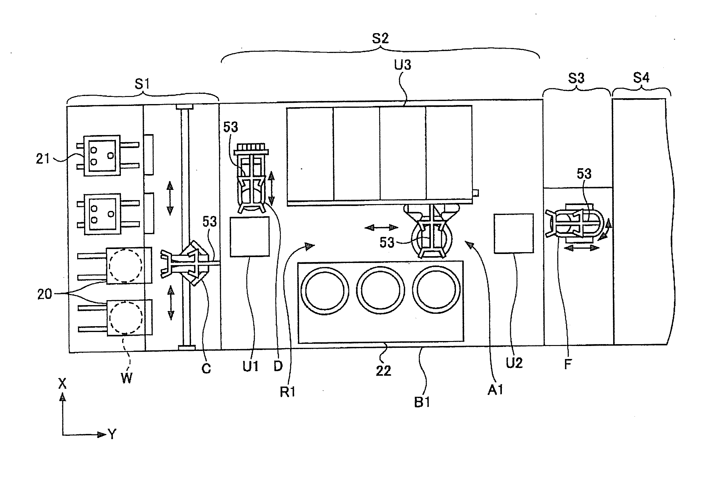
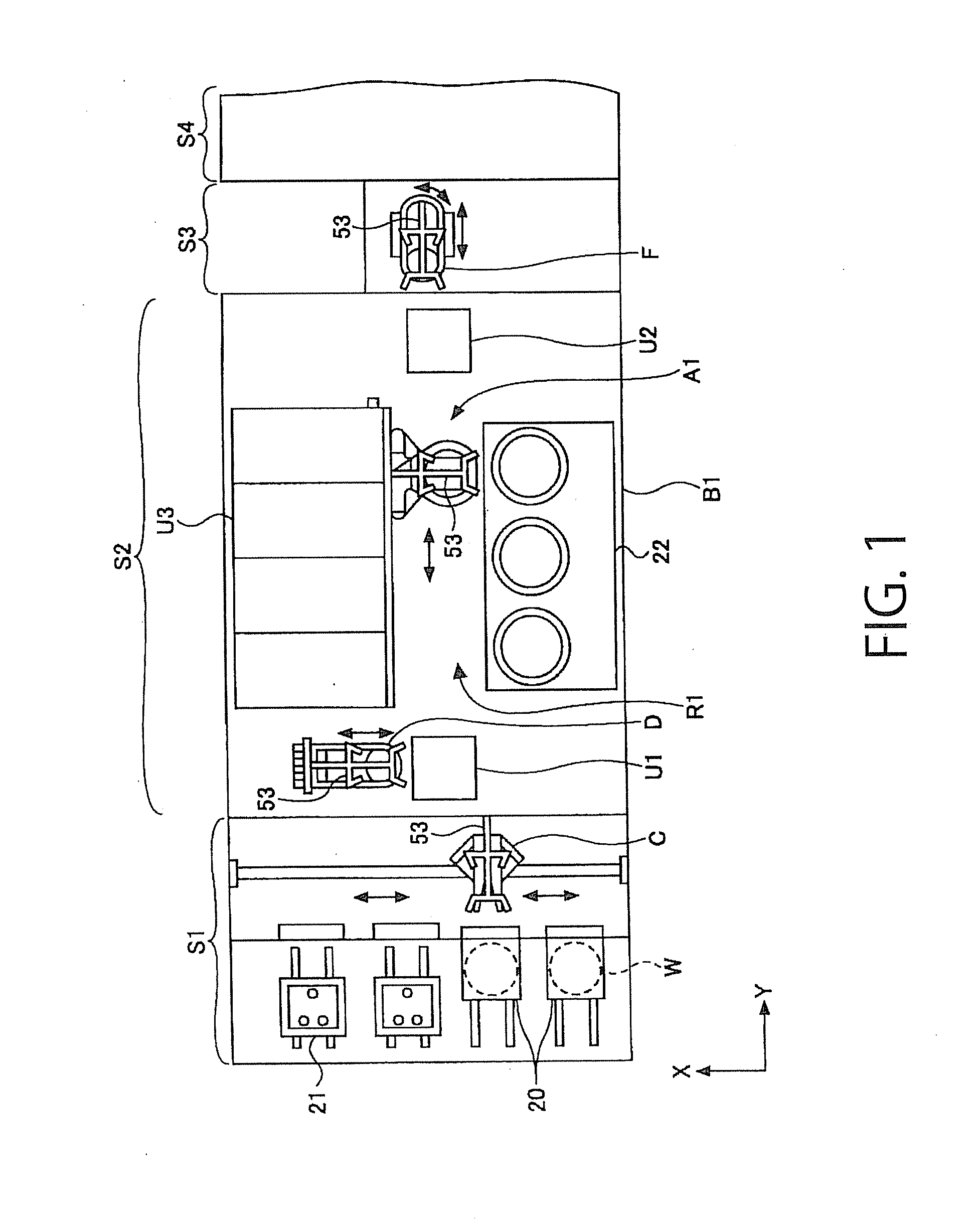
[0048]A resist pattern forming system built by connecting an exposure system to a coating and developing system, namely, a substrate processing system relating to a first embodiment according to the present embodiment will be briefly described with reference to FIGS. 1 to 4.
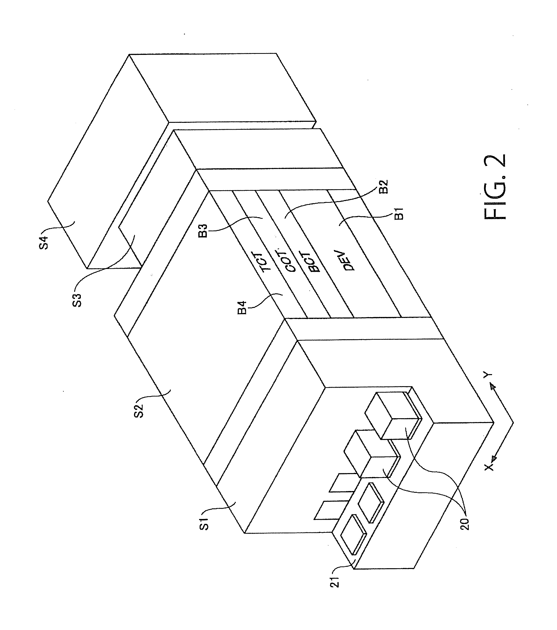
[0049]FIG. 1 is a plan view of a resist pattern forming system relating to the first embodiment. FIG. 2 is a schematic perspective view of the resist pattern forming system relating to the first embodiment. FIG. 3 is a side view of the resist pattern forming system relating to the first embodiment. FIG. 4 is a perspective view of a third unit, namely a COT layer.
[0050]Referring to FIGS. 1 and 2, the resist pattern forming system has a carrier block S1, a processing block S2 and an interface block S3. An exposure system S4 is connected to the interface block S3 of the resist pattern forming system. The carrier block S1, the processing block S2, the interface block S3 and the exposure system S4 are arranged and con...
second embodiment
[0168]A substrate processing method relating to a second embodiment according to the present embodiment will be described with reference to FIGS. 23 to 25.
[0169]A substrate processing method relating to the second embodiment is different from the substrate processing method relating to the first embodiment in that the holding fork is moved relative to the detecting units when any one of the detecting units detects a notch WN in a wafer W.
[0170]The substrate processing method is carried out also by the resist pattern forming system in the first embodiment built by combining the substrate processing system and the exposure system and hence the description of the substrate processing system will be omitted.
[0171]The substrate processing system is provided, similarly to the substrate processing system in the first embodiment, with four detecting units 5. The number of the necessary detecting units 5 is three or greater. Therefore, one of the four detecting units 5 may be omitted.
[0172]F...
first modification
of Second Embodiment
[0199]A substrate processing method in a first modification of the second embodiment according to the present embodiment will be described with reference to FIG. 26.
[0200]The substrate processing method in this modification is different from the substrate processing method in the second embodiment in that the holding fork is moved relative to the detecting units during the intermodule transfer step in which a wafer W is moved to the succeeding processing module when any one of the detecting units detects the notch WN of the wafer W.
[0201]A substrate processing method in this modification is the same as the substrate processing method in the first embodiment and is carried out by the resist pattern forming system built by connecting the exposure system to the coating and developing system and hence the description of the substrate processing system will be omitted.
[0202]This modification, similarly to the second embodiment, needs at least three detecting units 5 a...
PUM
 Abstract
Description
Claims
Application Information