Photovoltaic cell

Inactive Publication Date: 2012-03-08
TATUNG UNIVERSITY +1
View PDF25 Cites 7 Cited by
  • Summary
  • Abstract
  • Description
  • Claims
  • Application Information

AI Technical Summary

Benefits of technology

[0006]In order to overcome the above-mentioned problems, one object of the present invention is to provide a photovoltaic cell, which uses a wide bandgap material to allow the transmission of most photons (i.e. almost no photons being absorbed by the wide bandgap material). That is

Problems solved by technology

However, the inner N layer 12 is too thick and thus incident light cannot efficiently achieve the PN junction 121, resulting in loss of light.
The large thickness of the N layer 12 and the increased defects cause the difficult movement and ea

Method used


Image

  • Photovoltaic cell
  • Photovoltaic cell
  • Photovoltaic cell

Examples


Example

[0025]Exemplary embodiments will now be described in detail with reference to the accompanying drawings to make the Examiner be aware of features and effects of the present invention. In all drawings, the same reference numerals in the drawings denote identical or like elements, and thus their description will be omitted.

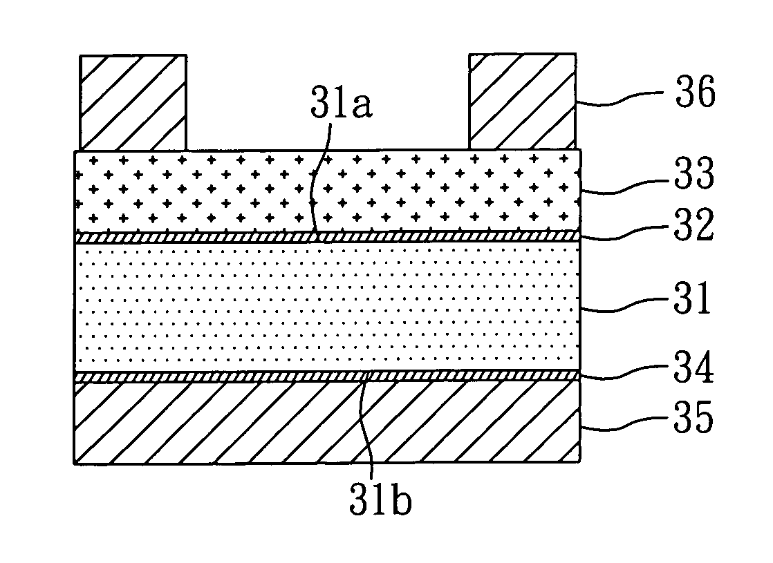
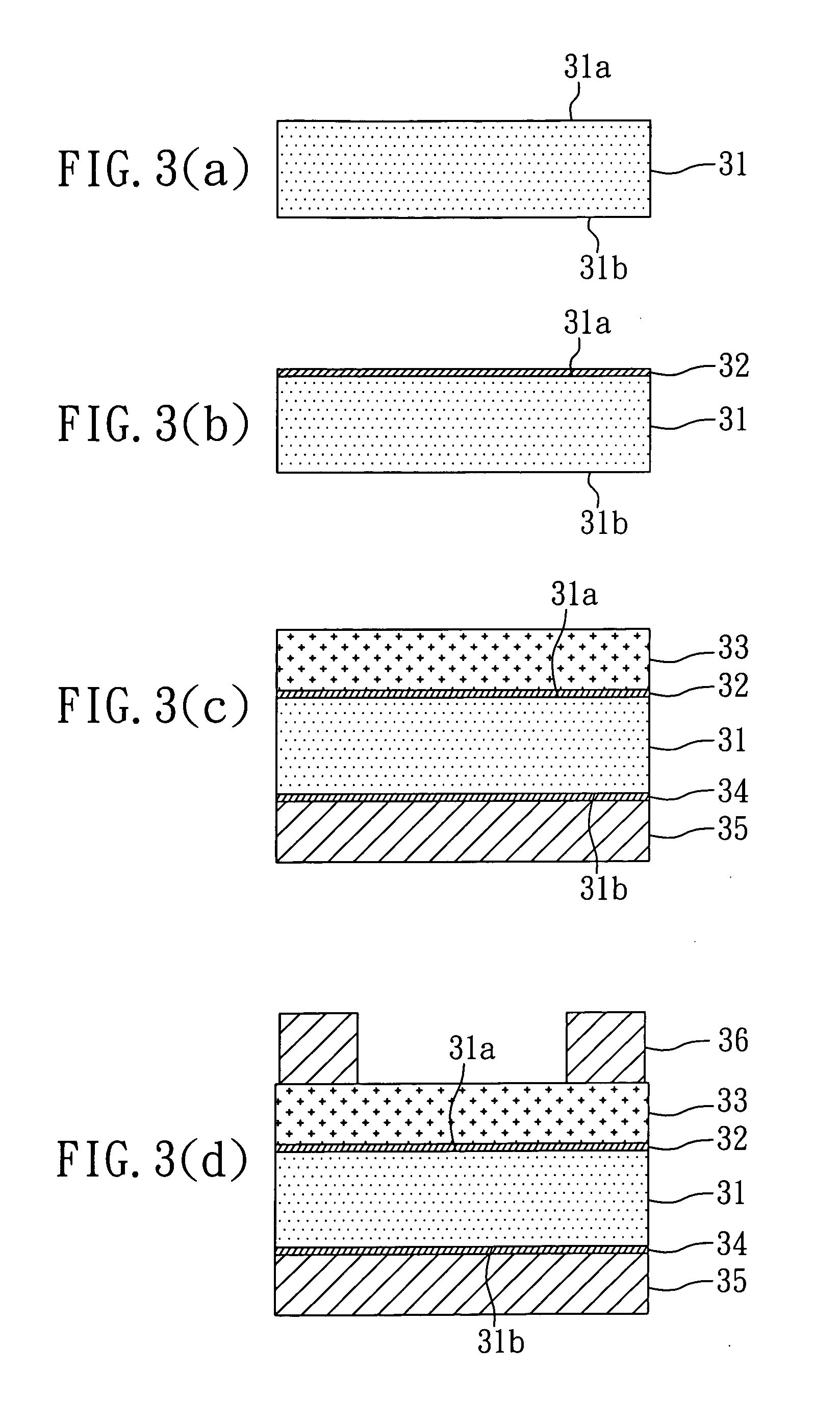
[0026]FIGS. 3(a) to 3(d) show a process for fabricating a photovoltaic cell according to one embodiment of the present invention. The photovoltaic cell includes:

[0027]a first bandgap layer 31 having a first surface 31a and a second surface 31b, in which a P-type silicon wafer is used and the bandgap of the P-type silicon wafer is 1.12 eV;

[0028]a second bandgap layer 32, which is a semiconductor film with a thickness of about 10 Å and may be an amorphous silicon film selected from anyone of an intrinsic semiconductor, an N-type semiconductor and a P-type semiconductor but is not limited to an amorphous silicon film, in which other similar films with a similar bandgap...


PUM


Abstract

A structure of photovoltaic cell for improving conversion efficiency has been disclosed, including a first bandgap layer, a second bandgap layer, a third bandgap layer, a back electrode and a finger electrode, wherein the first bandgap layer is a wafer while the second bandgap layer is a semiconductor film with a thickness of 1˜100 Å and a greater bandgap than one of the first bandgap layer, and the third bandgap layer comprises wide bandgap materials and a greater bandgap than one of the second bandgap layer. Thereby, the lattice mismatch of heterostructures between the first bandgap layer and the third bandgap layer may be solved by the second bandgap layer. Also, the carrier recombination within devices may be decreased and the output photocurrent may thus be enhanced to improve energy conversion efficiency.

Description

BACKGROUND OF THE INVENTION[0001]1. Field of the Invention[0002]The present invention relates to a photovoltaic cell and, more particularly, to a photovoltaic cell with a bandgap gradient.[0003]2. Description of Related Art[0004]Recently, renewable energy technologies have been promoted, and the industry mainly focuses on development of solar cells due to that solar cells may be used to supply energy in the future. Accordingly, solar cells for the development of solar energy are one of photovoltaic technologies having development potential in 21 century. FIG. 1 shows a conventional solar cell in a P-N junction structure, which includes: a finger electrode 10, a window layer 11, an N layer 13, a P-type silicon wafer 13 and a back electrode 14. The window layer 11 covers the surface of the N layer 12 to allow more incident photons to enter the interior of the solar cell. However, the inner N layer 12 is too thick and thus incident light cannot efficiently achieve the PN junction 121, ...

Claims


Application Information

Patent Timeline
IPC IPC(8): H01L31/06
CPCH01L31/0747Y02E10/547H01L31/20H01L31/1804Y02P70/50
Inventor LIN, CHIUNG-WEICHEN, YI-LIANG
Owner TATUNG UNIVERSITY
Why Eureka
Try Eureka