

Method and Chemistry for Selenium Electrodeposition
- Summary
- Abstract
- Description
- Claims
- Application Information
AI Technical Summary
Problems solved by technology
Method used
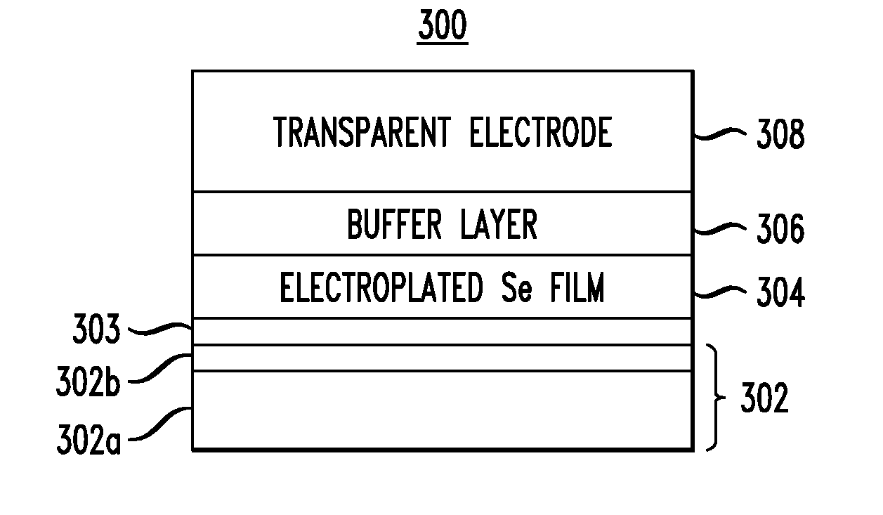
Image

Examples
Embodiment Construction
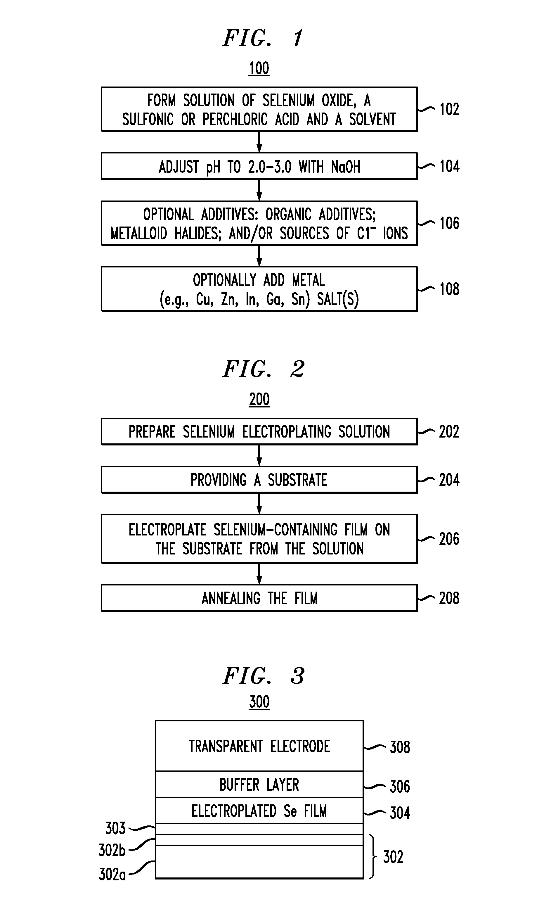
[0042]Provided herein are techniques that remedy the above-described problems associated with electrodepositing selenium (Se) films. The terms “electrodeposition” and “electroplating” are being used interchangeably herein. FIG. 1, for example, is a diagram illustrating an exemplary methodology 100 for preparing a Se electroplating solution. In step 102, the solution is formed from a mixture of selenium oxide, a sulfonic acid or perchloric acid (HClO4) and a solvent.
[0043]Any form of selenium oxide may be used. According to an exemplary embodiment, the selenium oxide is selenium dioxide (SeO2). Suitable sulfonic acids include, but are not limited to, alkane sulfonic acid (e.g., methane sulfonic acid (MSA)), alkene sulfonic acid, aryl sulfonic acid, heterocyclic sulfonic acid and aromatic sulfonic acid.
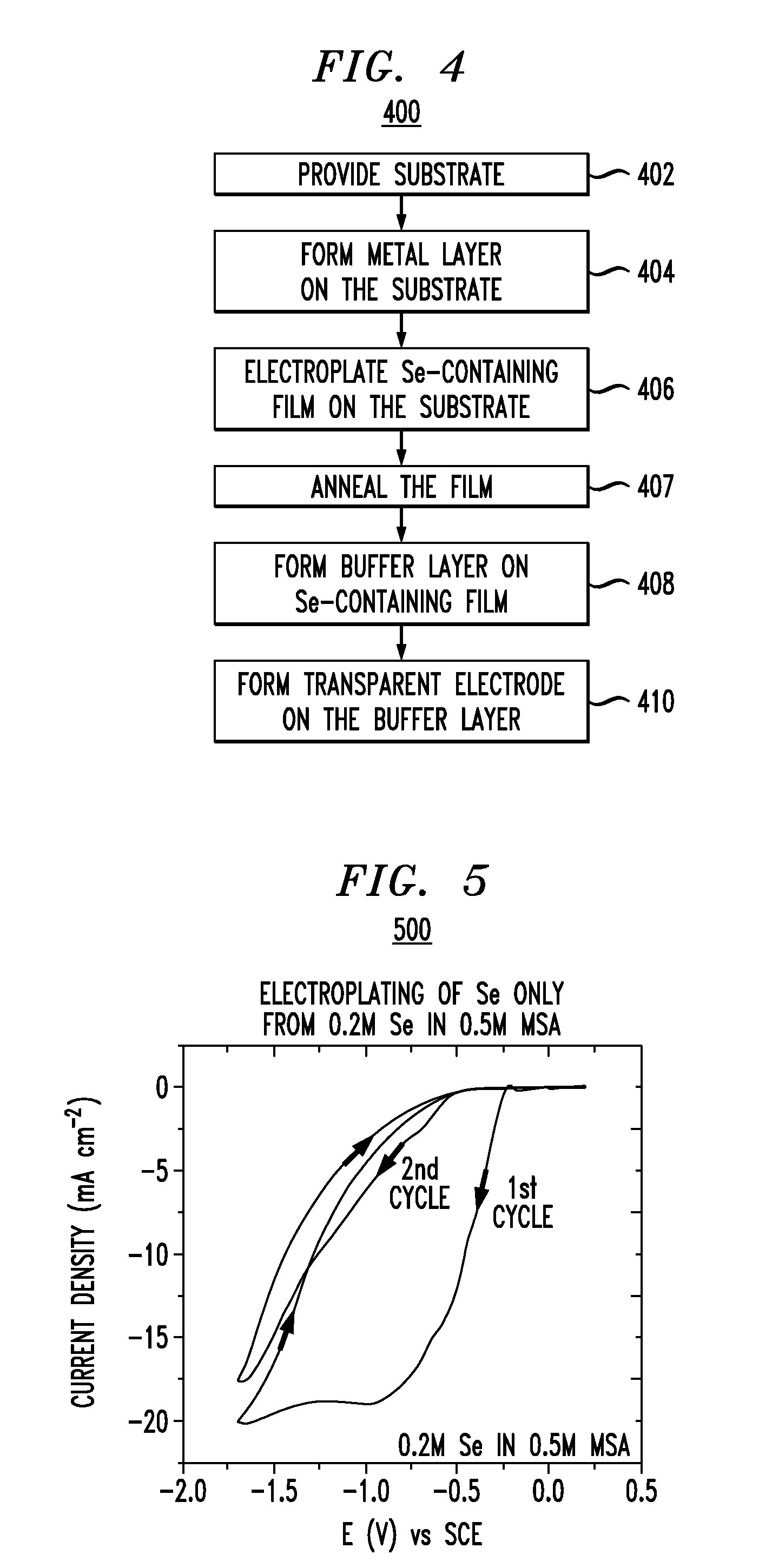
[0044]While either a sulfonic acid or HClO4 may be used in the electroplating solution, the sulfonic acid tends to perform better, see below. With all other acids tested, only a powdery...
PUM
| Property | Measurement | Unit |
|---|---|---|
| Temperature | aaaaa | aaaaa |
| Temperature | aaaaa | aaaaa |
Abstract
Description
Claims
Application Information