Magnetic antenna and board mounted with the same
a technology of magnetic antenna and board, applied in the field of magnetic antenna, can solve the problems of loss of antenna sensitivity, and achieve the effects of low production cost, stable joining, and low variation
- Summary
- Abstract
- Description
- Claims
- Application Information
AI Technical Summary
Benefits of technology
Problems solved by technology
Method used
Image
Examples
example 1
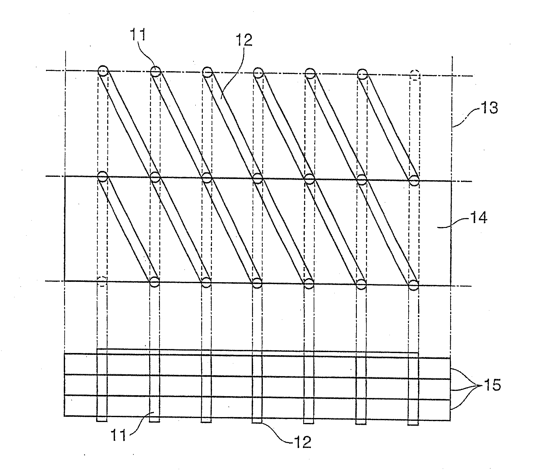
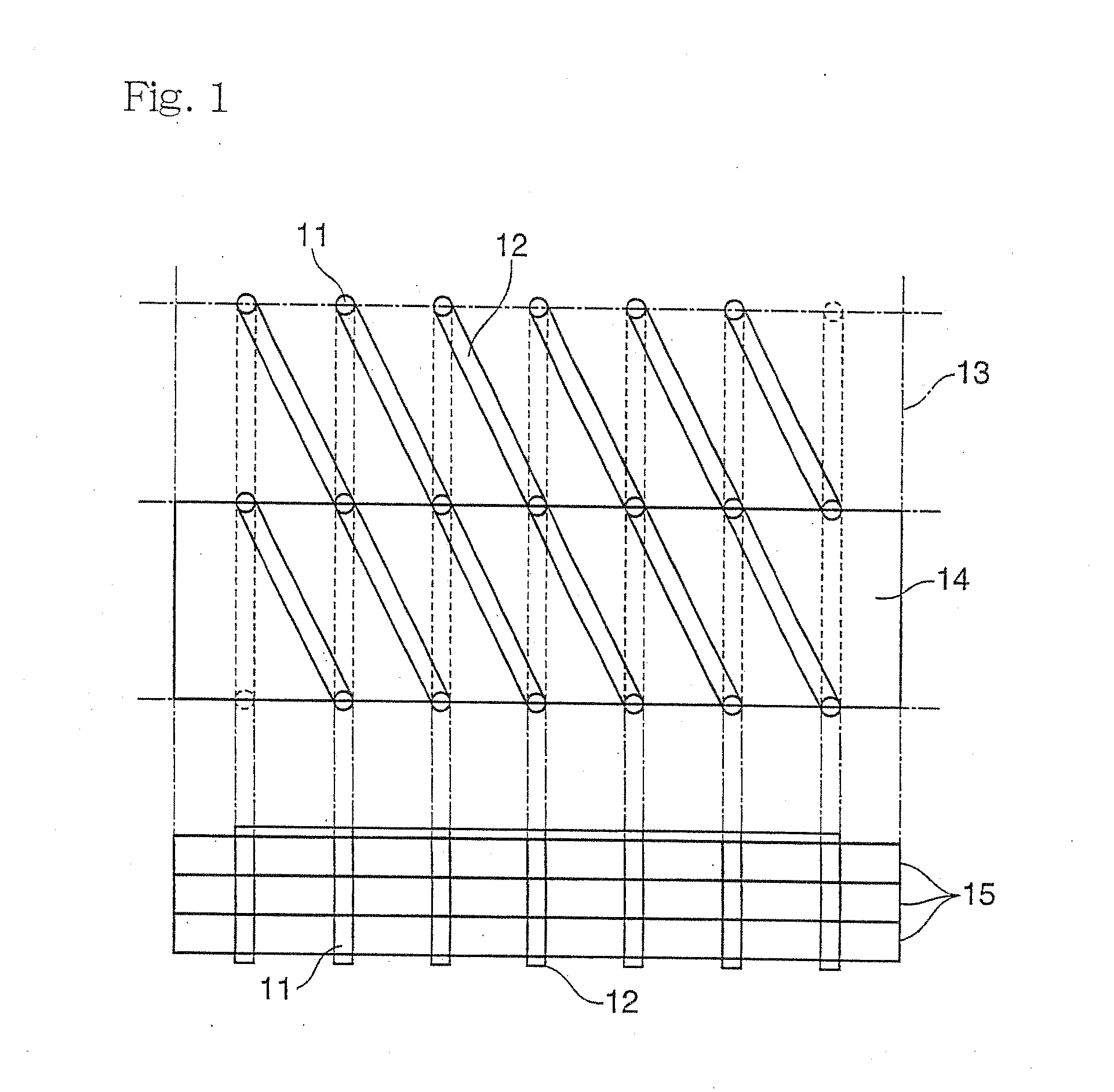
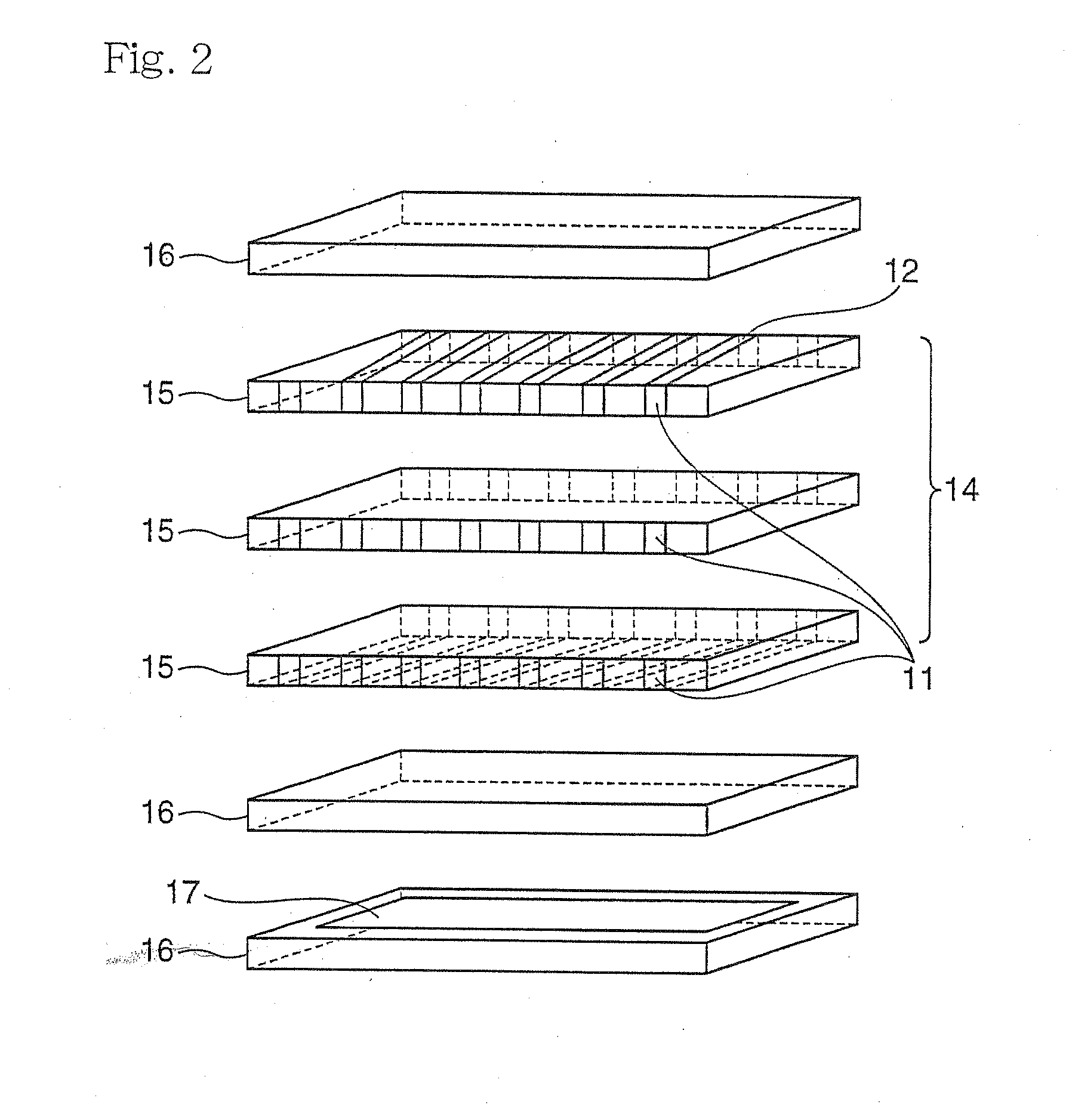
[0091]A magnetic antenna of the present invention was produced using an LTCC technology. First, a magnetic layer 15 was prepared. 100 Parts by weight of a calcined Ni—Zn—Cu ferrite powder which had been found to have a magnetic permeability of 100 at 13.56 MHz upon calcination at 900° C. (Fe2O3: 48.5 mol %, NiO: 25 mol %, ZnO: 16 mol %, CuO: 10.5 mol %), 8 parts by weight of a butyral resin, 5 parts by weight of a plasticizer, and 80 parts by weight of a solvent were mixed in a ball mill to prepare a slurry. The slurry was applied on PET films with a size of 150 mm×150 mm by a doctor blade to such a thickness that the resulting layer thickness after calcination would be 0.1 mm.
[0092]Insulating layers 16 were prepared as follows. 100 Parts by weight of a calcined Zn—Cu ferrite powder (Fe2O3: 48.5 mol %, ZnO: 41 mol %, CuO: 10.5 mol %), 8 parts by weight of a butyral resin, 5 parts by weight of a plasticizer, and 80 parts by weight of a solvent were mixed in a ball mill to prepare a s...
example 2
[0100]The same green sheets for the magnetic layer 15 as in Example 1, and green sheets comprising a glass ceramic, instead of a Zn—Cu ferrite, for the insulating layers 16 were used. As shown in FIG. 3, five green sheets for the magnetic layer 15 were stacked on top of one another, and through-holes 11 were formed therethrough and filled with an Ag paste. Then, an Ag paste was printed on the surfaces of the laminate perpendicular to the through-holes 11 to form coils 14.
[0101]A green sheet for an insulating layer 16 was stacked on one surfaces of the coils 14. At this time, a conductive layer 17 was printed on the insulating layer 16 with an Ag paste. Another insulating layer 16 was stacked on the other surfaces of the coils 14, and through-holes 11 were formed through the other insulating layer 16 in connection with both ends of the coils 14 and filled with an Ag paste. Coil lead terminals 19 and IC chip connecting terminals 18 to which an IC was connectable were printed on the ou...
example 3
[0104]The same green sheets for the magnetic layer 15 and the same green sheets for the insulating layers 16 as in Example 1 were used. As shown in FIG. 4, five green sheets for the magnetic layer 15 were stacked on top of one another, and through-holes 11 were formed therethrough and filled with an Ag paste. Then, an Ag paste was printed on the surfaces of the laminate perpendicular to the through-holes 11 to form coils 14.
[0105]A green sheet for an insulating layer 16 was stacked on the lower surfaces of the coils 14. At this time, a conductive layer 17 was printed on the insulating layer 16 with an Ag paste. A green sheet for a magnetic layer 15 was stacked on the lower surface of the insulating layer 16. A green sheet for another insulating layer 16 was stacked on the upper surfaces of the coils 14, and through-holes 11 were formed in the upper surface of the other insulating layer 16 in connection with both ends of the coils 14 and filled with Ag paste. Coil lead terminals 19 a...
PUM
 Abstract
Description
Claims
Application Information


