Method of designing an integrated circuit based on a combination of manufacturability, test coverage and, optionally, diagnostic coverage

Inactive Publication Date: 2012-03-15
GLOBALFOUNDRIES INC
View PDF7 Cites 11 Cited by
  • Summary
  • Abstract
  • Description
  • Claims
  • Application Information

AI Technical Summary

Benefits of technology

[0006]More particularly, in one embodiment of the design method, DFM modifications to the layout of an integrated circuit can be made in light of test coverage. Specifically, a set of test patterns for testing an integrated circuit can be generated, based on a description (e.g., a netlist for the integrated circuit). Next, test coverage can be determined and, more specifically, nodes covered by the test patterns (i.e., tested nodes) and nodes not covered by the test patterns (i.e., untested nodes) can be identified. Additionally, the description of the integrated circuit can be converted to a layout of the integrated circuit. Finally, modifications can be made to the layout, based on a set of design-for-manufacturability (DFM) rules, which specify different application requirements for the untested nodes as compared to the test nodes. For example, a particular DFM rule can require mandatory application to all of the untested nodes, but only discretionary application to the tested nodes. Another particular DFM rule can require application to any untested nodes at a higher priority than to any tested nodes.
[0007]In another embodiment of the integrated circuit design method, rather than making DFM modifications to the layout of an integrated circuit in light of test coverage, as described above, test coverage can be established in light of DFM modifications. Specifically, a description of the integrated circuit (e.g., a netlist for the integrated circuit) can be converted to a layout of the integrated circuit. Then, based on a set of design-for-manufacturability (DFM) rules, modifications can be to the layout. After the modifications are made to the layout, modified nodes and unmodified nodes in the integrated circuit can be identified. Finally, based on the description of the integrated circuit, a set of test patterns for testing the integrated circuit can be generated with test coverage for the unmodified nodes having a higher priority than test coverage for the modified nodes.
[0008]Alternatively, rather than basing DFM modifications on test coverage or establishing test coverage based on DFM modifications, an iterative process can be performed, for example, where DFM modifications to the layout of an integrated circuit are made in light of test coverage and then test coverage is altered in light of the DFM modifications. Specifically, a first set of test patterns for testing an integrated circuit can be

Problems solved by technology

It should be noted, however, that even with DFT modifications, 100% test coverage (e.g., test coverage of all nodes in an integrated circuit) is typically cost prohibitive, limited by design, test feasibility, and

Method used


Image

  • Method of designing an integrated circuit based on a combination of manufacturability, test coverage and, optionally, diagnostic coverage
  • Method of designing an integrated circuit based on a combination of manufacturability, test coverage and, optionally, diagnostic coverage
  • Method of designing an integrated circuit based on a combination of manufacturability, test coverage and, optionally, diagnostic coverage

Examples


Example

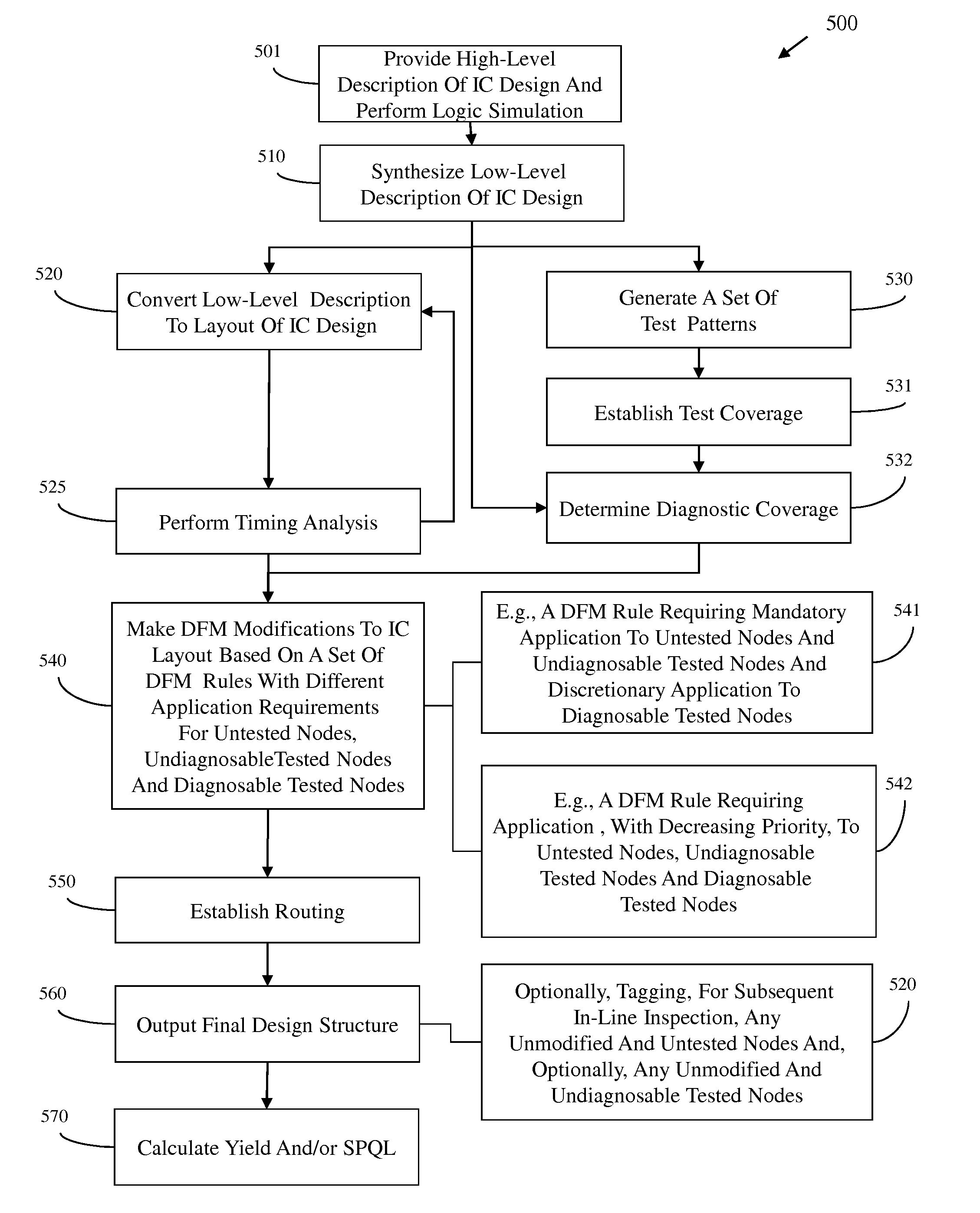
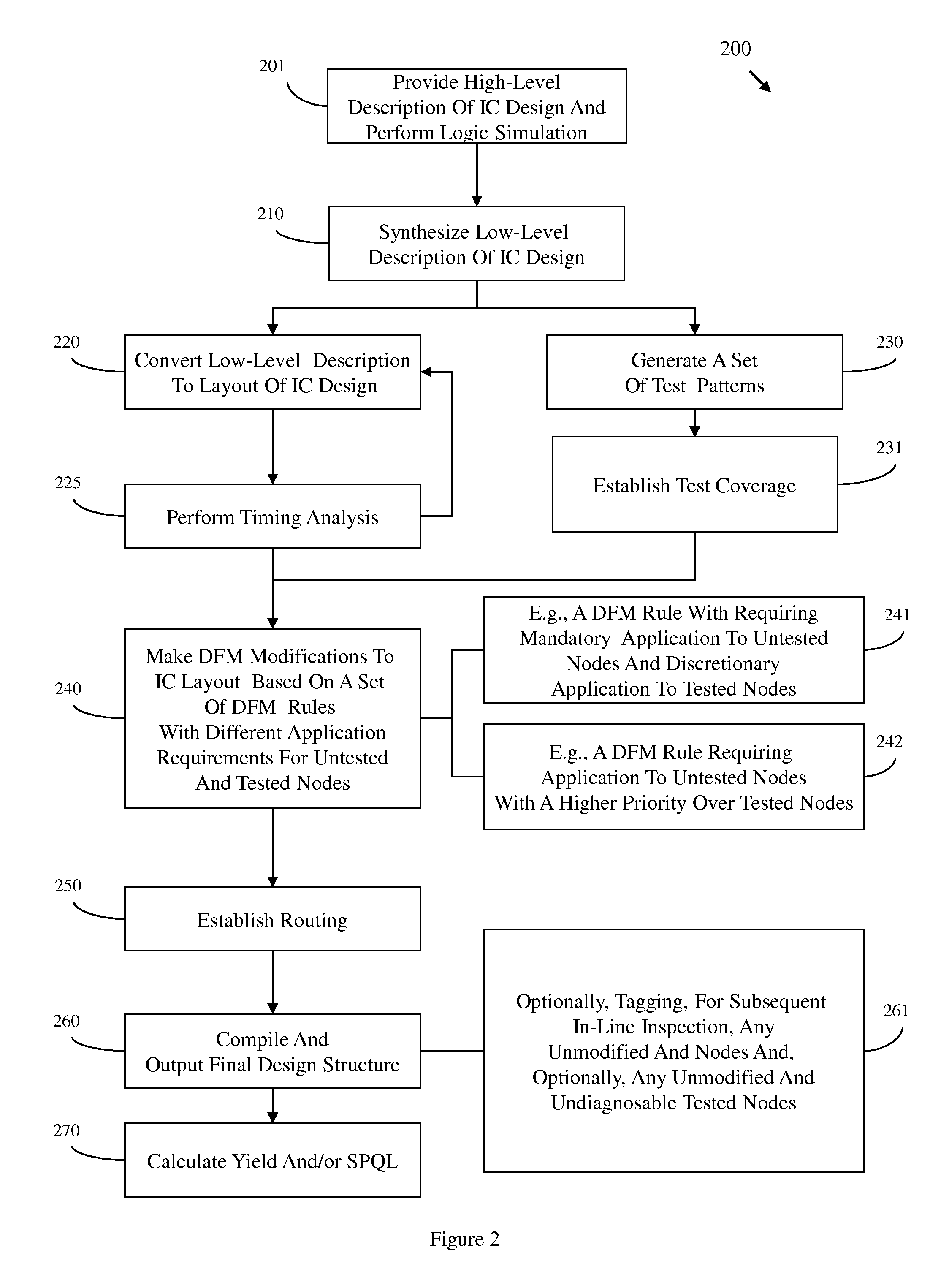
[0018]The embodiments of the invention and the various features and advantageous details thereof are explained more fully with reference to the non-limiting embodiments that are illustrated in the accompanying drawings and detailed in the following description.

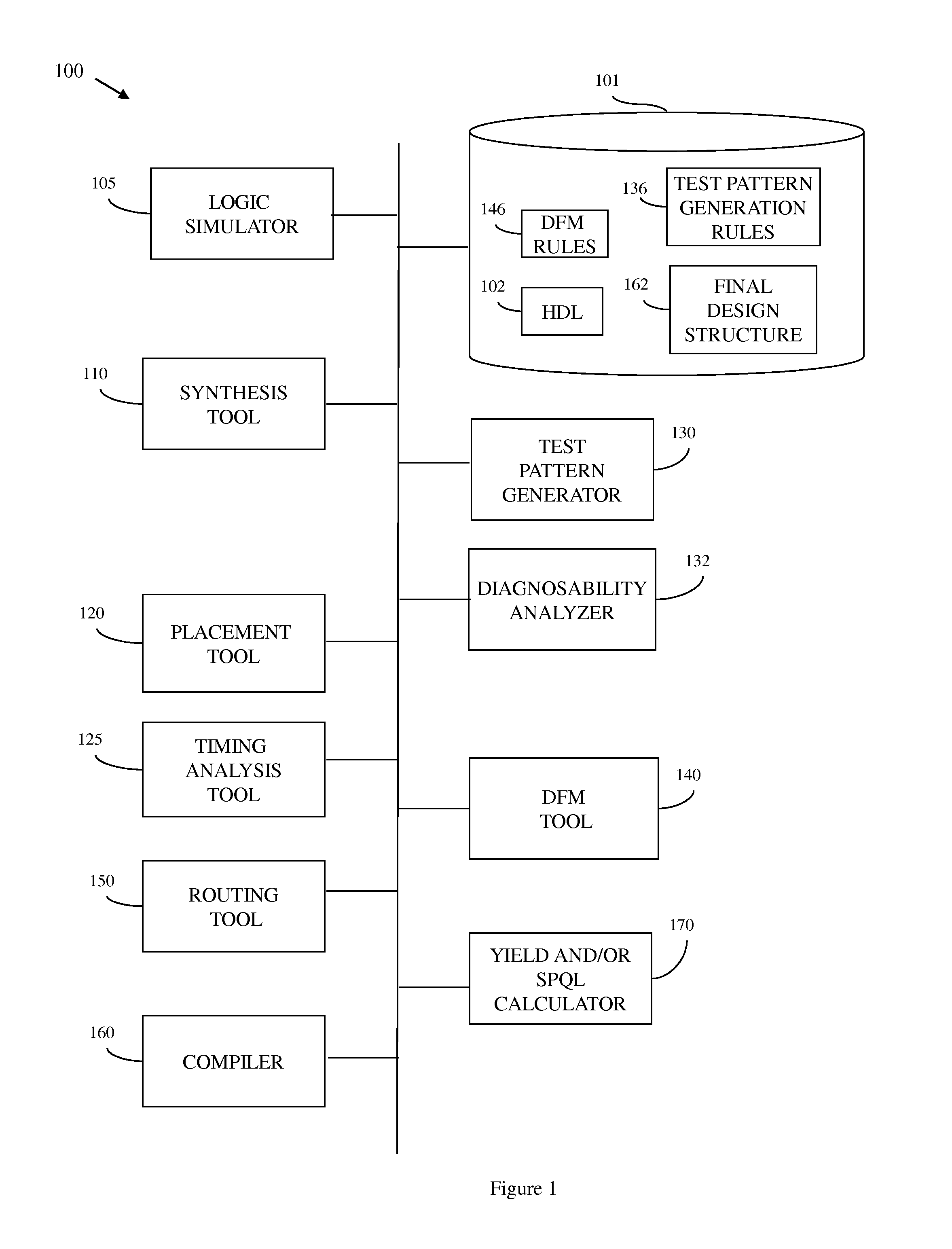
[0019]Integrated circuit design methods typically begin with a high-level description of the integrated circuit. This high-level description sets out the requirements for the integrated circuit and is stored on a data storage device in, for example, a hardware description language (HDL), such as VHDL or Verilog. Next, a logic synthesis tool (i.e., a synthesis engine) accesses the data storage device and synthesizes the high-level description into a low-level description of the integrated circuit chip (e.g., a gate-level netlist). Based on this low-level description, a placement tool establishes placement for devices on an integrated circuit chip or, more particularly, placement of groups of interconnected devices, referred to ...


PUM


Abstract

Disclose are embodiments of an integrated circuit design method based on a combination of manufacturability, test coverage and, optionally, diagnostic coverage. Design-for manufacturability (DFM) modifications to the layout of an integrated circuit can be made in light of test coverage. Alternatively, test coverage of an integrated circuit can be established in light of DFM modifications. Alternatively, an iterative process can be performed, where DFM modifications to the layout of an integrated circuit are made in light of test coverage and then test coverage is altered in light of the DFM modifications. Alternatively, DFM modifications to the layout of an integrated circuit can be made in light of test coverage and also diagnostic coverage. In any case, after making DFM modifications and establishing test coverage, any unmodified and untested nodes (and, optionally, any unmodified and undiagnosable tested nodes) in the integrated circuit can be identified and tagged for subsequent in-line inspection.

Description

BACKGROUND[0001]1. Field of the Invention[0002]The embodiments relate to integrated circuit design methods and, more particularly, to an integrated circuit design method based on a combination of manufacturability, test coverage and, optionally, diagnostic coverage.[0003]2. Description of the Related Art[0004]Integrated circuit design methods often incorporate both design-for-manufacturability (DFM) techniques and design-for-testability (DFT) techniques. DFM techniques typically involve making modifications to the layout of an integrated circuit based on a pre-established set of rules to improve the manufacturability of the integrated circuit (i.e., to improve yield and / or reliability of the integrated circuit, as manufactured). For example, DFM modifications can be made to enhance elements of individual cells, to enhance higher-level routing (e.g., by increasing wire widths and / or by providing redundant vias), to enhance memory redundancy, to increase spacing between wires or vias,...

Claims


Application Information

Patent Timeline
IPC IPC(8): G06F17/50G06F9/455
CPCG06F2217/12G06F17/5045G06F30/30G06F2119/18Y02P90/02
Inventor BERNSTEIN, KERRYCULP, JAMES A.PASTEL, LEAH M.P.PETERSON, KIRK D.ROHRER, NORMAN J.
Owner GLOBALFOUNDRIES INC
Why Eureka
Try Eureka