Group iii nitride nanorod light emitting device and method of manufacturing thereof

a technology of nitride nanorods and light-emitting devices, which is applied in the manufacture of semiconductor/solid-state devices, semiconductor devices, electrical devices, etc., can solve the problems of deteriorating luminous efficiency, increasing the driving voltage of devices, and degrading the operating characteristics of devices, so as to minimize the defects generated during the growth of single crystal nanorods and improve the three-dimensional structure

Active Publication Date: 2012-03-22
SAMSUNG ELECTRONICS CO LTD
View PDF2 Cites 64 Cited by
  • Summary
  • Abstract
  • Description
  • Claims
  • Application Information

AI Technical Summary

Benefits of technology

[0007]An aspect of the present invention provides a group III nitride nanorod light emitting device in which crystal defects generated during the growing of a single cry

Problems solved by technology

In general, in a case in which a group III nitride nanorod is grown above a substrate, properly controlling the diameter, length, growth position, and crystal growth direction of the nanorod may be difficult, thereby causing difficulties in forming a nanorod having a desired shape and generating defects, wher

Method used


Image

  • Group iii nitride nanorod light emitting device and method of manufacturing thereof
  • Group iii nitride nanorod light emitting device and method of manufacturing thereof
  • Group iii nitride nanorod light emitting device and method of manufacturing thereof

Examples


Embodiment Construction

[0032]Exemplary embodiments of the present invention will now be described in detail with reference to the accompanying drawings. The invention may, however, be embodied in many different forms and should not be construed as being limited to the embodiments set forth herein. Rather, these embodiments are provided so that this disclosure will be thorough and complete, and will fully convey the scope of the invention to those skilled in the art. While those skilled in the art could readily devise many other varied embodiments that incorporate the teachings of the present invention through the addition, modification or deletion of elements, such embodiments may fall within the scope of the present invention.

[0033]The same or equivalent elements are referred to by the same reference numerals throughout the specification.

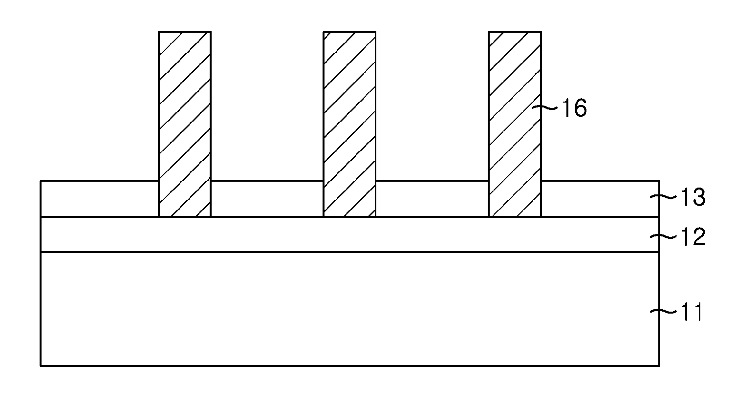
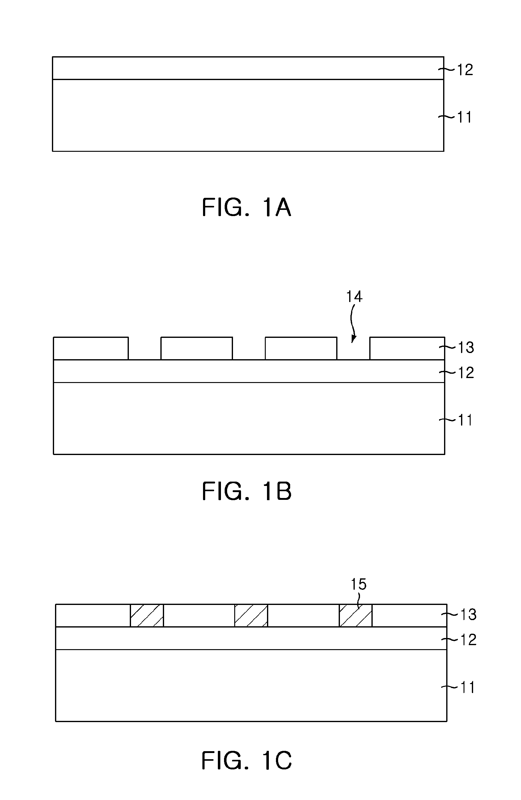
[0034]FIGS. 1A through 1D are diagrams showing a process of forming first conductive group III nitride nanorods above a substrate according to an exemplary embodiment of...


PUM


Abstract

A group III nitride nanorod light emitting device and a method of manufacturing thereof. The method includes preparing a substrate, forming an insulating film including one or more openings exposing parts of the substrate on the substrate, growing first conductive group III nitride nanorod seed layers on the substrate exposed through the openings by supplying a group III source gas and a nitrogen (N) source gas thereto, growing first conductive group III nitride nanorods on the first conductive group III nitride nanorod seed layers by supplying the group III source gas and an impurity source gas in a pulse mode and continuously supplying the N source gas, forming an active layer on a surface of each of the first conductive group III nitride nanorods, and forming a second conductive nitride semiconductor layer on the active layer.

Description

CROSS-REFERENCE TO RELATED APPLICATIONS[0001]This application claims the priority of Korean Patent Application No. 10-2010-0090115 filed on Sep. 14, 2010, in the Korean Intellectual Property Office, the disclosure of which is incorporated herein by reference.BACKGROUND OF THE INVENTION[0002]1. Field of the Invention[0003]The present invention relates to a group III nitride nanorod, and more particularly, to a light emitting device using the group III nitride nanorod and a method of manufacturing thereof.[0004]2. Description of the Related Art[0005]In general, in a case in which a group III nitride nanorod is grown above a substrate, properly controlling the diameter, length, growth position, and crystal growth direction of the nanorod may be difficult, thereby causing difficulties in forming a nanorod having a desired shape and generating defects, whereby the driving voltage of a device is increased and the operating characteristics of the device are degraded.[0006]In particular, in...

Claims


Application Information

Patent Timeline
IPC IPC(8): H01L33/04H01L33/32
CPCH01L33/08H01L33/32H01L33/24H01L33/16H01L33/0062
Inventor SEONG, HAN KYUCHUNG, HUN JAEYANG, JUNG JASONE, CHEOL SOO
Owner SAMSUNG ELECTRONICS CO LTD
Why Eureka
Try Eureka