Sector Array Addressing for ECC Management

a technology of ecc management and sector arrays, applied in information storage, static storage, digital storage, etc., can solve the problems of data integrity damage, flash memory cells are potentially subject to a number of errors that affect data integrity, and may originate bit errors, so as to reduce the effect of data integrity damage and reduce the number of memory cells

Active Publication Date: 2012-03-22
OVONYX MEMORY TECH LLC
View PDF4 Cites 31 Cited by
  • Summary
  • Abstract
  • Description
  • Claims
  • Application Information

AI Technical Summary

Benefits of technology

[0015]This invention provides an addressing scheme for electronic memory arrays that manages error correction. The addressing scheme is well suited to arrays that contain configuration defects such as short circuits or open circuits between row and/or column lines. The addressing scheme minimizes the effect of a confi

Problems solved by technology

Volatile memory suffers from the disadvantage, however, that its data content is lost when the memory is powered down.
Flash memory cells are potentially subject to a number of errors that affect data integrity.
Bit errors may originate from access operations, configuration defects in the array, or a combination of the two.
Errors originating from access operations occur through errors in the access protocol or when a correct access protocol induces unintended effects in the array.
Configuration defects are structural defects and include problems such as short circuits and open circuits caused by defects in the memory elements in the array or addressing and drive elements (transistors, diodes, and interconnect).
Configuration defects may occur at the time of manufacture or develop over time through use of the array.
Bit errors include write errors, write-disturb errors, data retention errors (caused by leakage of charge from the floating gate), read errors, and read-disturb errors.
As the number of states utilized in flash memory increases, the detection margin for the different states narrows and the technology becomes more susceptible to errors and the need to correct errors becomes more pressing.
As efforts toward chip miniaturization continue, the scaling of flash memory to smaller dimensions is becoming increasingly problematic.
Problems include difficulties in reliably fabricating ever thinner oxide regions for separating the floating gate from both the substrate and the control gate and loss of margin in read and write operations.
A reduction in charge makes detection of charge more demanding and is especially problematic in multilevel designs because it becomes increasingly

Method used


Image

  • Sector Array Addressing for ECC Management
  • Sector Array Addressing for ECC Management
  • Sector Array Addressing for ECC Management

Examples


Embodiment Construction

[0028]Although this invention will be described in terms of certain preferred embodiments, other embodiments that are apparent to those of ordinary skill in the art, including embodiments that do not provide all of the benefits and features set forth herein, are also within the scope of this invention. Accordingly, the scope of the invention is defined only by reference to the appended claims.

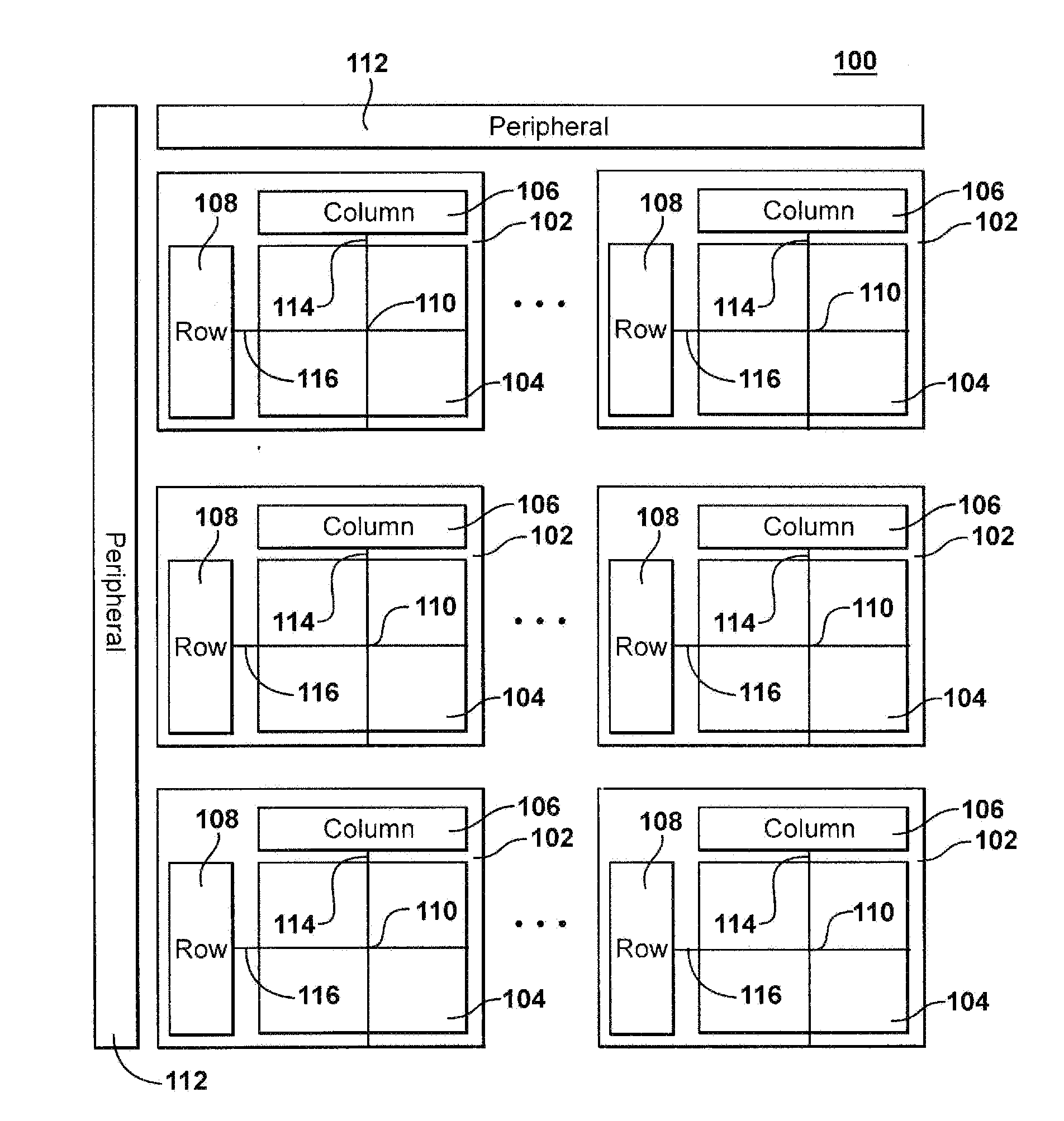
[0029]This invention provides an addressing scheme for electronic memory arrays. The addressing scheme is especially adapted to keeping the demands of error correction to within limits of the ECC method used to analyze and correct the data stored or fetched. In one embodiment, the demands of error correction are maintained within the error correction capabilities of a conventional flash controller. By managing error correction to maintain compatibility with a standard flash controller, commercial adoption of promising non-volatile alternatives to flash memory is expected to be facilitated and t...


PUM


Abstract

An addressing scheme for non-volatile memory arrays having short circuit defects that manages the demand for error correction. The scheme generally avoids simultaneous active driving of the row line and column line of the selected cell during write. Instead, only a single row or column line is actively driven at any one time and all other array lines are left floating. In addition, the number of memory cells accessed from a given row or column during a fetch may be limited. The benefits of the scheme include preventing short circuits from drawing excess currents through the array and limiting the frequency of read or write failures caused by short circuits to a manageable number. In one embodiment, the scheme maintains the demand for error correction to within the error correction capability of a flash controller. Exemplary embodiments include phase-change memory arrays.

Description

FIELD OF INVENTION[0001]This invention relates to error correction in an electronic memory array. More particularly, this invention relates to error correction in an electronic memory array that includes short circuit defects. Most particularly, this invention minimizes the number of cells subject to read or write errors as a consequence of short circuit defects.BACKGROUND OF THE INVENTION[0002]Electronic memory is widely used in consumer and commercial applications. The different types of electronic memory are broadly classified as volatile or non-volatile. Volatile memory includes SRAM and DRAM and is advantageous because it provides fast reading and writing operations (SRAM) and high density (DRAM). Volatile memory suffers from the disadvantage, however, that its data content is lost when the memory is powered down. Non-volatile memory, in contrast, retains its data when powered down. Non-volatile memory includes EPROM, EEPROM, and Flash. As markets have expanded, volatile and no...

Claims


Application Information

Patent Timeline
IPC IPC(8): G11C11/22G11C7/00G11C11/00
CPCG11C11/22G11C13/0033G11C13/0023G11C13/0004
Inventor PARKINSON, WARDTRENT, THOMAS
Owner OVONYX MEMORY TECH LLC
Why Eureka
Try Eureka