Transmissive Body

a resistive device and body technology, applied in the field of input devices, can solve the problems of resistive devices that can also be sensitive to humidity, require excessive power usage, and dim the underlying screen, and achieve the effects of reducing system complexity and cost, and reducing the width of the bezel

Inactive Publication Date: 2012-04-26
ZETTA RES & DEV LLC RPO SERIES
View PDF8 Cites 65 Cited by
  • Summary
  • Abstract
  • Description
  • Claims
  • Application Information

AI Technical Summary

Benefits of technology

[0077]To avoid the necessity of having to carefully position a single LED point light source, a small array of individually controllable LEDs may be used and the apparatus configured to activate only the best-located LED to achieve optimal collimated light, which is preferably parallel to the focal axis (or simply the ‘axis’) of the collimation element. During the production phase of an apparatus comprising the transmissive body of the invention, a computer algorithm can be used to test for which of the individual LEDs or combination of LEDs gives the best system performance. This will generally correspond to the LED that is at the focus (or focal point), or combination of LEDs that cover the focal point. The additional cost of including a small LED array as opposed to a single LED point light source is offset by the flexibility such a configuration provides. Of course, it will be appreciated that precise positioning of a point source of light is less important when the transmissive body of the invention is being utilised to direct light into an assembly for illuminating a display, as described in WO 08 / 138,049 A1.
[0085]The advantage of this latter embodiment is that a single collimation element can be used to generate a pair of sheets of collimated light that propagate at an angle relative to each other. Preferably the sheets of light are in the same plane (i.e. coplanar) or in closely spaced parallel planes. As discussed above, mirrors can be used to reflect the off-axis light back towards appropriately positioned / angled detectors, or appropriately positioned / angled waveguides to receive and collect light. In this way, it is possible to determine a touch location in two dimensions since there are two intersecting sheets of light. Besides the advantage of only requiring a single collimation element, this embodiment also offers significantly reduced bezel width on the sides having the mirrors. Further advantages will be apparent in a reduction in system complexity and cost. It will be appreciated that when this embodiment is used in an input device the mirrors will have to be placed parallel to the sides of the input area and the receive waveguides will need to be angled appropriately to receive light from a respective sheet of light produced by the transmissive body according to this embodiment of the invention.
[0087]In further embodiments, it is possible to include three point sources of light, for example one positioned at the focus of the collimation element and the other two at two corners of the transmissive element. In this way three sheets of light are generated, each propagating in a different direction. The skilled person will appreciate that this embodiment provides an efficient means for resolving the so-called double touch ambiguity often encountered in infrared touch input devices.

Problems solved by technology

The most common approach uses a flexible resistive overlay, although the overlay is easily damaged, can cause glare problems, and tends to dim the underlying screen, requiring excess power usage to compensate for such dimming.
Resistive devices can also be sensitive to humidity, and the cost of the resistive overlay scales quadratically with perimeter.
In this case the overlay is generally more durable, but the glare and dimming problems remain.
They have the advantage of being overlay-free and can function in a variety of ambient light conditions (U.S. Pat. No. 4,988,983), but have a significant cost problem in that they require a large number of source and detector components, as well as supporting electronics.
Since the spatial resolution of such systems depends on the number of sources and detectors, this component cost increases with display size and resolution.
Firstly, because touch functionality is being increasingly common in consumer electronics devices such as mobile phones, handheld games and personal digital assistants (PDAs), there is a continuing requirement to reduce costs. Even if relatively inexpensive waveguide materials and fabrication techniques (such as curable polymers patterned by a photolithographic or moulding process) are used, the transmit and receive waveguide arrays still represent a significant fraction of the cost of the touch input device.
Secondly there is a signal-to-noise problem: because the transmit waveguides are small (typically they have a square or rectangular cross section with sides of order 10 μm), it is difficult to couple a large amount of ‘signal’ light into them from the optical source. Since only a fraction of this light will be captured by the receive waveguides, the system as a whole is vulnerable to ‘noise’ from ambient light, especially if used in bright sunlight.
Thirdly, because the device uses discrete beams 12, the transmit and receive waveguides need to be carefully aligned during assembly. A similar alignment requirement applies to the older infrared touch input devices with arrays of discrete sources and detectors.
This will further reduce the Bill of Materials, and possibly also the assembly costs.
However it has the significant disadvantage of being a complicated design, with numerous sharp corners and concave portions that will be extremely difficult to reproduce accurately via injection moulding.
A second problem is that, analogous to the well-known principle of single slit diffraction, the divergence angle of a light beam reflected off a facet will depend on the height of that facet.
Unfortunately this simple configuration has the disadvantage that in many parts of the input area, a touch object 60 will block the outgoing light 35, complicating the detection algorithms.
A known problem with this form of device is relatively poor spatial resolution in the portion of the input area close to the edge 208 between the two optical units.
Hybrid infrared / optical touch input devices where arrays of optical fibres around the edges of a rectangular input area receive light from optical sources in the corners are also known, see for example PCT Patent Application Publication No WO 2008 / 130145 A1, but these can likewise suffer from relatively poor spatial resolution close to one or more of the edges.

Method used


Image

  • Transmissive Body
  • Transmissive Body
  • Transmissive Body

Examples


Embodiment Construction

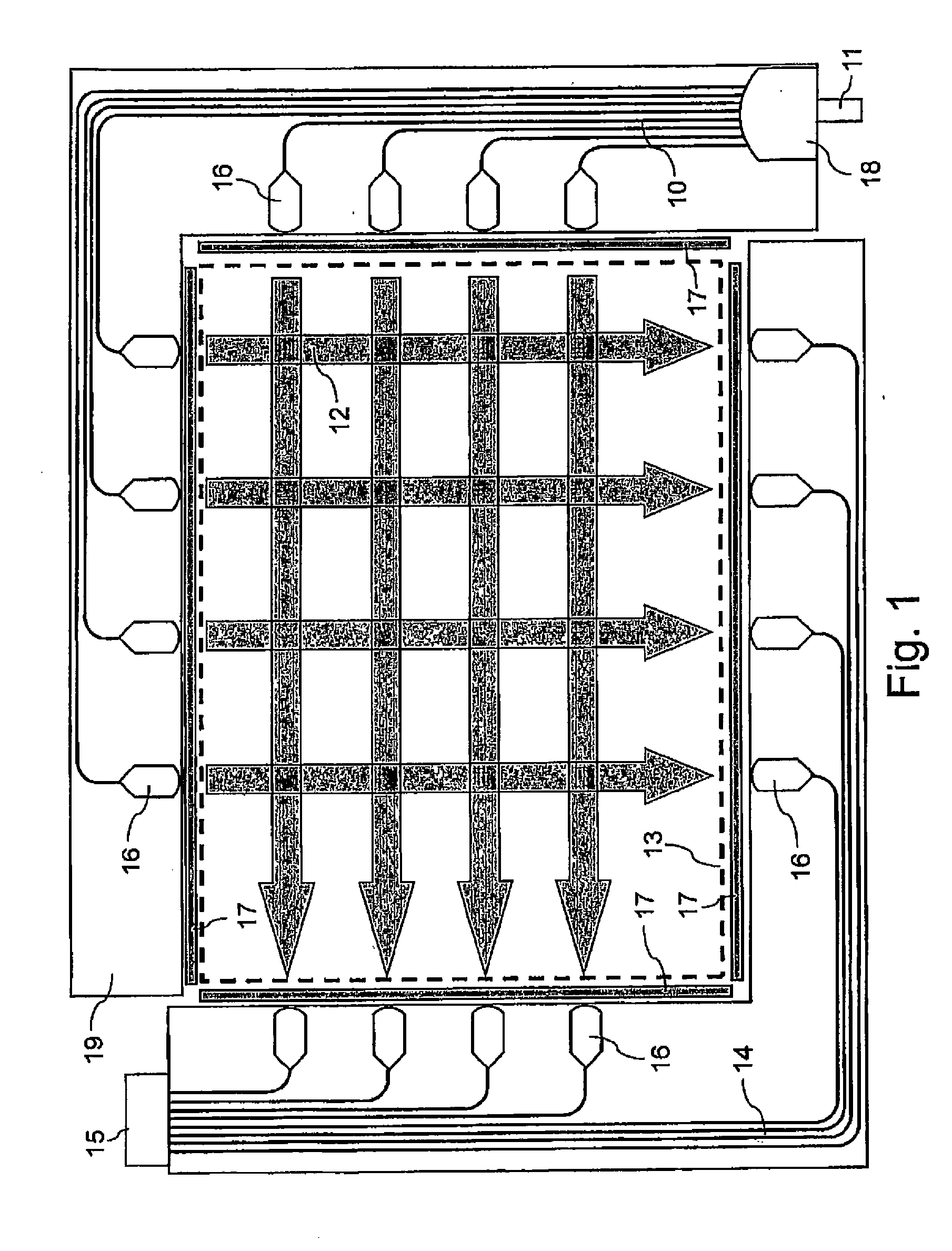
[0188]References will now be made to the drawings wherein like reference numerals refer to like parts throughout. As mentioned previously, waveguide-based optical touch screen sensors of the type shown in FIG. 1 tend to suffer from a signal to noise problem, where their performance is impaired in bright ambient light conditions. There is also a need to reduce costs, especially in the arrays of transmit waveguides 10 and receive waveguides 14, and to avoid the requirement to align the transmit and receive waveguides carefully during assembly.

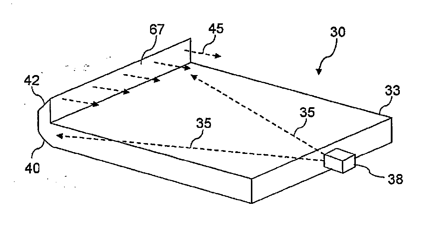
[0189]FIGS. 3, 4 and 5 show plan, side and perspective views respectively of a substantially planar transmissive body 30 for an input device according to a first embodiment of the invention. The transmissive body 30 comprises a transmissive element 33 adapted to receive, confine and transmit in planar form an optical signal 35 from an optical source 38. The transmissive body 30 further comprises a collimation element 40 adapted to substantially c...


PUM


Abstract

An apparatus and method for transmitting, collimating and redirecting light from a point-like source to produce a collimated optical signal in a substantially planar form are provided. In one embodiment the apparatus is manufactured as a unitary transmissive body comprising a collimation element and a redirection element, and optionally a transmissive element. In another embodiment the apparatus is assembled from one or more components. The apparatus and method are useful for providing sensing light for an optical touch input device.

Description

CROSS-REFERENCE TO RELATED APPLICATIONS[0001]This application claims priority to Australian provisional application No. 2008905605 filed on 31 Oct. 2008, which is incorporated herein by reference.[0002]This application is related to U.S. provisional patent application No. 60 / 917,567 filed May 11, 2007 and to U.S. provisional patent application No. 60 / 971,696 filed Sep. 12, 2007. This application is also related to Patent Co-Operation Treaty Patent Application No PCT / AU2008 / 000658 filed on May 12, 2008 and published as WO 08 / 138,049 A1. The contents of these applications are hereby incorporated herein by reference.FIELD OF THE INVENTION[0003]In certain embodiments the present invention relates to input devices, and in particular, optical touch input devices. In other embodiments the present invention relates to apparatus for illuminating a display. In further embodiments the present invention relates to combined input devices and apparatus for illuminating a display. However it will ...

Claims


Application Information

Patent Timeline
Patent Type & Authority Applications(United States)
IPC IPC(8): G06F3/042G02B27/42G02B27/30
CPCG02B6/0018G02B27/0983G06F3/0421G02B19/0028G06F2203/04109G02B19/0066G02B19/009G06F3/0428
Inventor KLEINERT, ANDREWROSS, DUNCAN IANPAYNE, JONATHANHOLLOWAY, WARWICK TODDATKINS, GRAHAM ROYCHARTERS, ROBERT BRUCECHONG, KENLIKUKULJ, DAXMAUND, BRIGGMAXWELL, IAN ANDREW
Owner ZETTA RES & DEV LLC RPO SERIES
Why Eureka
Try Eureka