Low on-resistance resurf mos transistor

a mos transistor, low on-resistance technology, applied in the field ofmos transistors, can solve the problems of corresponding increase in the surface on-resistance of the device, and achieve the effects of reducing the surface resistance of the resurf ldmos, reducing the breakdown voltage, and increasing the surface resistance of the mos transistor

Inactive Publication Date: 2012-05-03
MACRONIX INT CO LTD
View PDF4 Cites 38 Cited by
  • Summary
  • Abstract
  • Description
  • Claims
  • Application Information

AI Technical Summary

Benefits of technology

[0006]In view of the prior art, although a high breakdown voltage is provided by the P-top layer implanted in the conventional double or multi RESURF LDMOS for operating with high voltage, the P-top layer also causes the surface resistance of the RESURF LDMOS increases. Therefore, the present invention provides a RESURF MOS transistor not only has a high breakdown voltage but also provides a lower on-resistance than the conventional double RESURF LDMOS. The MOS provided by the present invention is in possession of two properties, the high breakdown voltage and the low resistance, at the same time.

Problems solved by technology

However, on the other hand, a drawback that the surface on-resistance of the device is increased is correspondingly induced since the carrier (electron) concentration at the upper portion of the HVNW 12 is decreased owing to the implanted P-top layer 16.

Method used


Image

  • Low on-resistance resurf mos transistor
  • Low on-resistance resurf mos transistor
  • Low on-resistance resurf mos transistor

Examples


Embodiment Construction

[0038]The present invention will now be described more specifically with reference to the following embodiments. It is to be noted that the following descriptions of preferred embodiments of this invention are presented herein for the purposes of illustration and description only; it is not intended to be exhaustive or to be limited to the precise form disclosed.

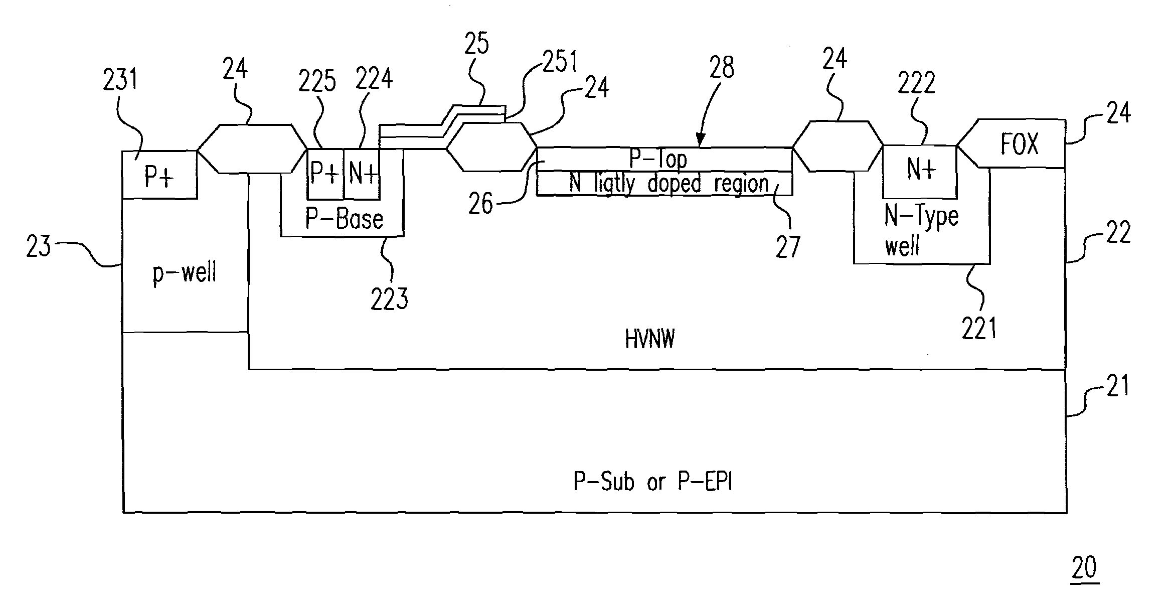
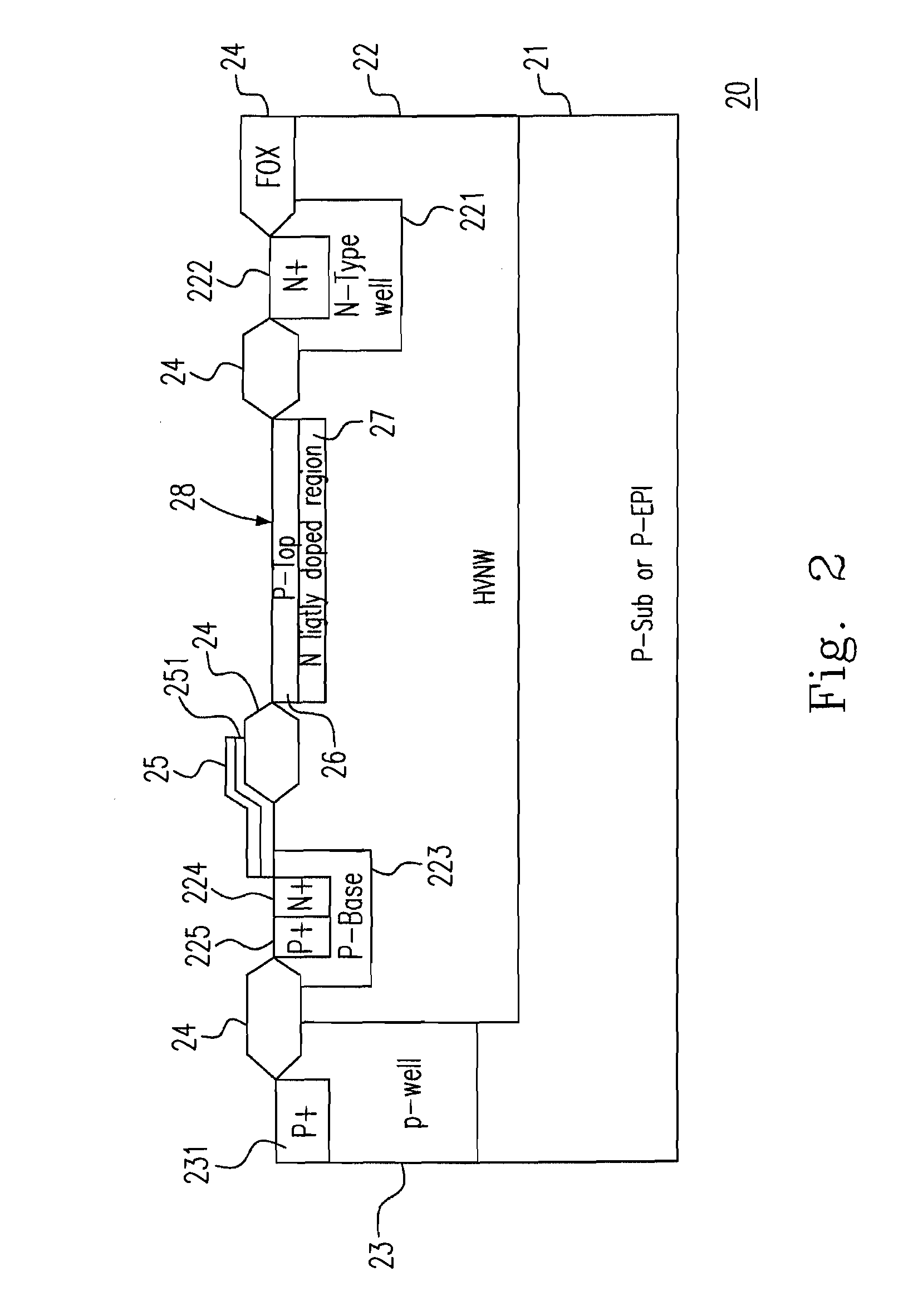
[0039]Please refer to FIG. 2, which is a cross section of an n-channel LDMOS for illustrating the first embodiment of the low on-resistance double RESURF MOS transistor according to the present invention. As shown in FIG. 2, the LDMOS 20 has a substrate 21, a high voltage N well (HVNW) 22, an N-type well 221, an N+ source region 224, a P-base 223, an N+ drain region 222, a P+ contact region 225, a P-well 23, a P+ region 231, isolation regions 24, a gate electrode 25, a gate oxide 251, a P-top layer 26, and an N lightly doped region 27.

[0040]The HVNW 22 and P-well 23 are formed in the upper portion of the substrate 21, wherei...


PUM


Abstract

The present invention relates to a low on-resistance RESURF MOS transistor, comprising: a drift region; two isolation regions formed on the drift region; a first-doping-type layer disposed between the two isolation regions; and a second-doping-type layer disposed below the first-doping-type layer.

Description

FIELD OF THE INVENTION[0001]The present invention relates to a MOS transistor, and more particularly to a low on-resistance RESURF MOS transistor.BACKGROUND OF THE INVENTION[0002]In recent years, lateral diffused MOSFET transistors (aka LDMOS) are widely used for operating under high voltage in very large scale integrated circuit (VLSI). For ascending the operating voltage of devices, the concept of REduced SURface Field (aka RESURF) have been widely used for power semiconductor devices development because it gives the best trade-off breakdown voltage and Rdson.[0003]FIG. 1 is a cross section of a conventional double RESURF n-channel LDMOS transistor 10. The double RESURF n-channel LDMOS transistor 10 has a P-type substrate 11, a high voltage N well (HVNW) 12, an N-type well 121, an N+ source region 124, a P-base 123, an N+ drain region 122, a P+ contact region 125, a P-well 13, a P+ region 131, isolation regions 14, a gate electrode 15 and a P-top layer 16.[0004]Due to the implante...

Claims


Application Information

Patent Timeline
Patent Type & Authority Applications(United States)
IPC IPC(8): H01L29/78H01L21/336
CPCH01L29/0634H01L29/0653H01L29/7835H01L29/0878H01L29/7816H01L29/0847H01L29/42368
Inventor CHU, CHIEN-WENCHAN, WING-CHORWU, SHYI-YUAN
Owner MACRONIX INT CO LTD
Why Eureka
Try Eureka