Topside structures for an insulated gate bipolar transistor (IGBT) device to achieve improved device performances

a technology of insulated gate bipolar transistor and topside structure, which is applied in the direction of semiconductor devices, basic electric elements, electrical appliances, etc., can solve the problems of high energy dissipation, high energy consumption, and high energy consumption of semiconductor devices, so as to improve injection and reduce e-on and e-off losses.

Active Publication Date: 2012-05-03
ALPHA & OMEGA SEMICON INC
View PDF4 Cites 65 Cited by
  • Summary
  • Abstract
  • Description
  • Claims
  • Application Information

AI Technical Summary

Benefits of technology

[0008]It is therefore an aspect of the present invention to provide a new and improved IGBT device configuration and manufacturing method for providing a trench IGBT device with a shielded gate IGBT with more heavily doped layer N layer such that the IGBT with can achieve increased injection with lower E-on and E-off losses.

Problems solved by technology

Conventional technologies to configure and manufacture insulated gate bipolar transistor (IGBT) devices are still confronted with difficulties and limitations to further improve the performances due to different tradeoffs.
A high Jsat will result in a lot of energy dissipated in the device during short circuit, which would quickly damage the IGBT device.
A lower Jsat will reduce the amount of energy dissipated, allowing the IGBT device to withstand the short circuit for a longer period of time without permanent damage; however, a lower Jsat also results in higher conductivity loss VCE,sat.
However the device can still have good conductivity because the lightly doped drift region undergoes high level carrier injection from the bottom P collector region resulting in its conductivity modulation.
The high Crss of this IGBT device slows down the device switching speed and also leads to higher switching energy losses. FIG. 1C is a cross sectional view of another conventional IGBT device.
However, such device has a lower breakdown voltage due to the heavily doped layer and has a further worsened Crss due to the heavily doped N-layer.

Method used


Image

  • Topside structures for an insulated gate bipolar transistor (IGBT) device to achieve improved device performances
  • Topside structures for an insulated gate bipolar transistor (IGBT) device to achieve improved device performances
  • Topside structures for an insulated gate bipolar transistor (IGBT) device to achieve improved device performances

Examples


Embodiment Construction

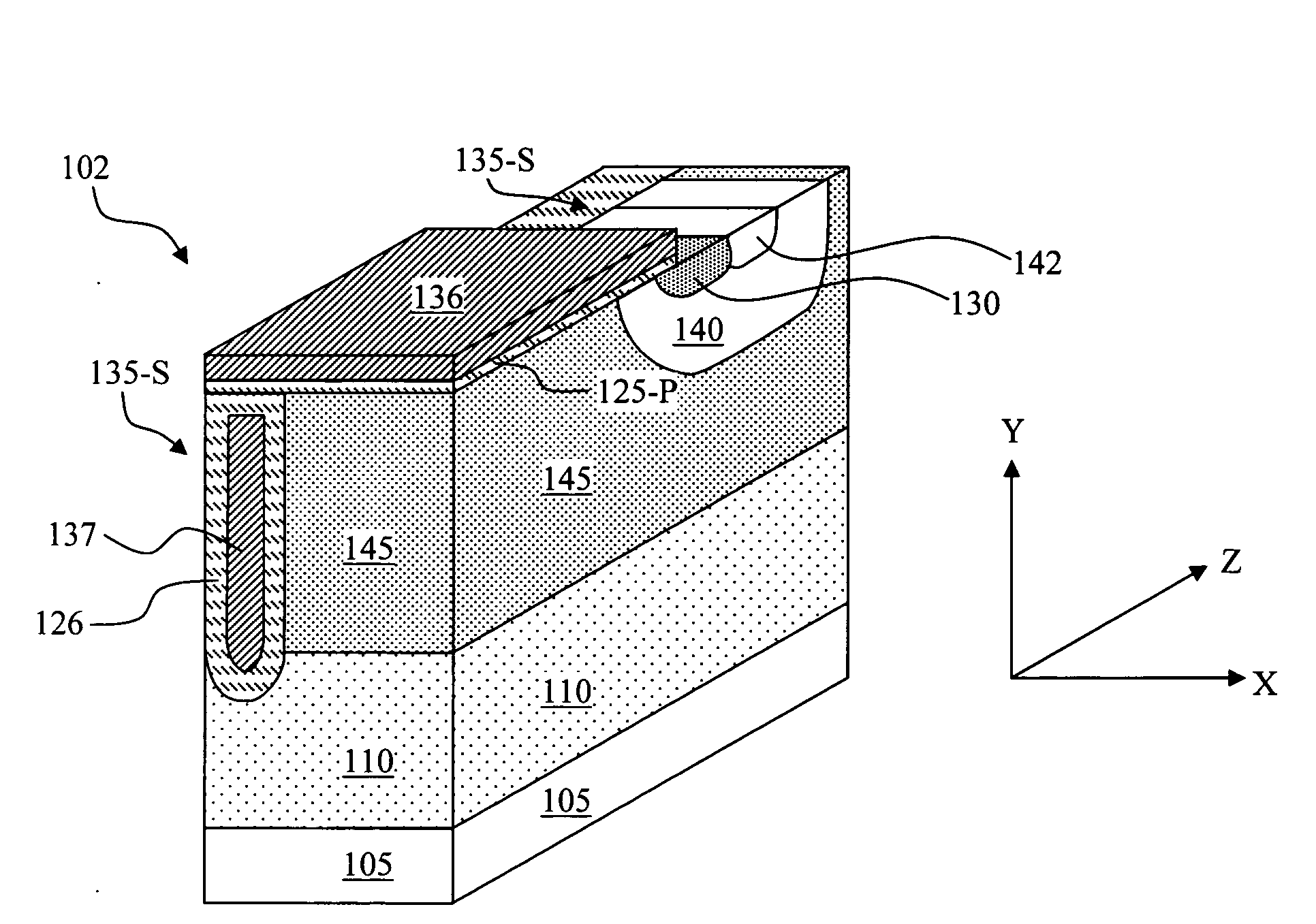
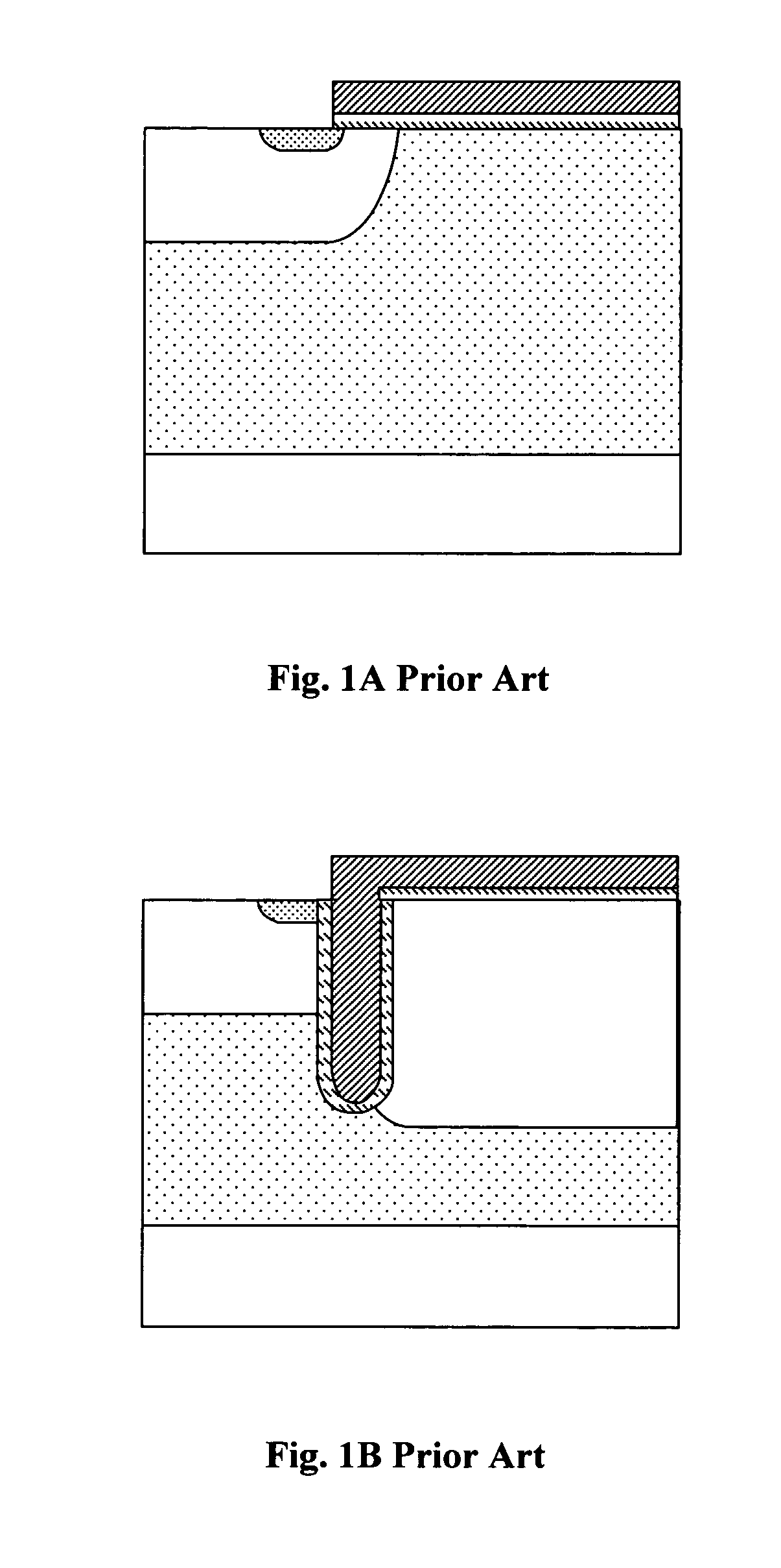
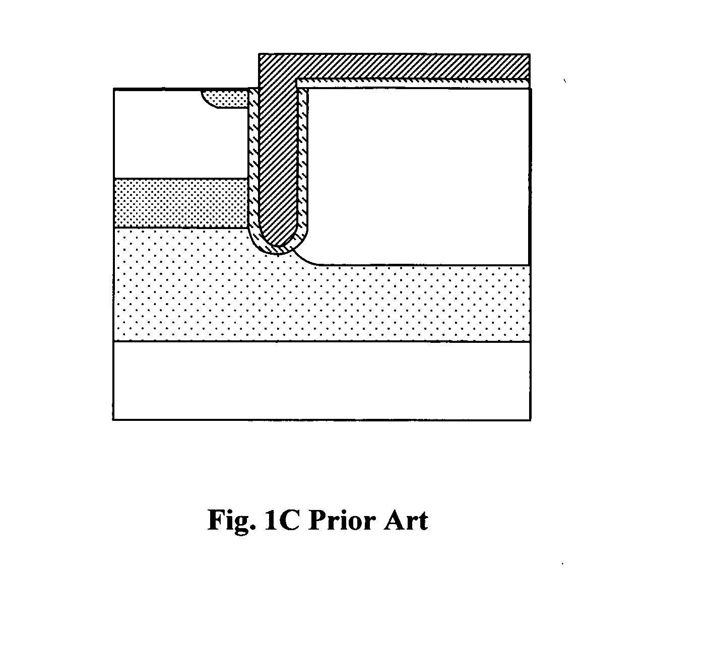
[0030]FIG. 2 is a cross-sectional view of an IGBT device having a trench shield and trench gate configuration with dummy trench of this invention. The IGBT device 100 is formed in semiconductor substrate 105 that has a first conductivity type, e.g., a P type substrate 105. An epitaxial layer 110 of a second conductivity type, e.g., an N-epitaxial (epi) layer 110, is supported on top of the P-type substrate, 105. Alternatively, the P type substrate 105 and the epitaxial layer 110 may together be referred to as the semiconductor substrate since they both generally have a monocrystalline structure; additionally, the P type substrate may be more generally referred to as a bottom or lower semiconductor layer and the epitaxial layer 110 may more generally be referred to as an upper semiconductor layer. The IGBT 100 is a vertical IGBT device with a collector electrode 120 disposed on a bottom surface of the substrate and an emitter electrode 131 disposed on a top surface. The IGBT device s...


PUM


Abstract

This invention discloses an insulated gate bipolar transistor (IGBT) device formed in a semiconductor substrate. The IGBT device has a split-shielded trench gate that includes an upper gate segment and a lower shield segment. The IGBT device may further include a dummy trench filled with a dielectric layer disposed at a distance away from the split-shielded trench gate. The IGBT device further includes a body region extended between the split-shielded trench gate and the dummy trench encompassing a source region surrounding the split-shielded trench gate near a top surface of the semiconductor substrate. The IGBT device further includes a heavily doped N region disposed below the body region and above a source-dopant drift region above a bottom body-dopant collector region at a bottom surface of the semiconductor substrate. In an alternative embodiment, the IGBT may include a planar gate with a trench shield electrode.

Description

BACKGROUND OF THE INVENTION[0001]1. Field of the Invention[0002]The invention relates generally to semiconductor power devices. More particularly, this invention relates to new configurations and methods for manufacturing improved device structures for insulated gate bipolar transistors (IGBT).[0003]2. Description of the Prior Art[0004]Conventional technologies to configure and manufacture insulated gate bipolar transistor (IGBT) devices are still confronted with difficulties and limitations to further improve the performances due to different tradeoffs. In IGBT devices, there is a tradeoff between the conduction loss VCE,sat (which depends upon the collector to emitter saturation voltage at rated current VCE,sat) and turn-off switching losses, Eoff. More carrier injection while the device is on improves the conductivity of the device, thus reducing conduction loss, but more carrier injection would also cause higher Eoff, because of the energy dissipated when clearing out the inject...

Claims


Application Information

Patent Timeline
Patent Type & Authority Applications(United States)
IPC IPC(8): H01L29/739H01L21/331
CPCH01L29/0696H01L29/7397H01L29/66348H01L29/402
Inventor BOBDE, MADHURBHALLA, ANUP
Owner ALPHA & OMEGA SEMICON INC
Why Eureka
Try Eureka