
Method for receiving frequency domain multiplexed signal and device for receiving frequency domain multiplexed signal

a frequency domain multiplexing and signal technology, applied in the direction of pulse manipulation, pulse technique, amplitude demodulation, etc., can solve problems such as character degradation, achieve high correlation, simplify the structure of the receiving device, and reduce the sampling frequency of an adc

Active Publication Date: 2012-05-03
NIPPON TELEGRAPH & TELEPHONE CORP
View PDF8 Cites 6 Cited by
  • Summary
  • Abstract
  • Description
  • Claims
  • Application Information

AI Technical Summary

Benefits of technology

[0041]According to an embodiment of the present invention, a digital signal acquisition step acquires digital signals from received signals that are multiplexed in the frequency domain. An offset discrete Fourier transform step applies an offset discrete Fourier transform to odd discrete point numbers based on the obtained digital signals. A decode step decodes frequency domain digital signals in the frequency domains obtained by the offset discrete Fourier transform, which are the frequency domain digital signals of one or more frequency channels.
[0042]As a result, in the case where a few frequency channels are received, even if the received signals are transformed into signals in the frequency domain using a Fourier transform, it is possible to select frequency channels corresponding to the transmitted signals appropriately. Furthermore, it is possible to reduce the sampling frequency of an ADC that acquires the signal position using a Fourier transform.
[0043]According to another embodiment of the present invention, a digital signal acquisition step acquires digital signals from the received signals that are multiplexed in a frequency domain. A branching step branches the obtained digital signals to frequency channel numbers for decoding. An initial coefficient storage step stores different coefficients with low correlation as initial weights with respect to each of the branched signal sequences. An equalization step equalizes each of the branched signal sequences using the different coefficients. A decode step decodes each of the equalized signal series.
[0044]As a result, it is possible to decode signals transmitted by an orthogonal frequency division multiplexing system without applying a discrete Fourier transform.
[0045]According to yet another embodiment of the present invention, a digital signal acquisition step acquires digital signals from received signals that are multiplexed in the frequency domain. A branching step branches the obtained digital signals to frequency channels for decoding. An initial coefficient storage step stores coefficients having high correlation with the coefficients of a discrete Fourier transform corresponding to each of the frequency channels, or coefficients including at least part of them, as initial weights with respect to each of the branched signal series. An equalization step equalizes the coefficients stored in the initial coefficient storage step as initial weights. A decode step decodes each of the equalized signal sequences.
[0046]As a result, since the received signals that are multiplexed in the frequency domain are equalized without a discrete Fourier transform, an individual discrete Fourier transform section for decoding the frequency channels can be omitted, so that it is possible to simplify the structure of the receiving device.

Problems solved by technology

In a frequency channel corresponding to a DC component, the characteristics deteriorate due to the influence of interference between signals and noise.

Method used


Image

  • Method for receiving frequency domain multiplexed signal and device for receiving frequency domain multiplexed signal
  • Method for receiving frequency domain multiplexed signal and device for receiving frequency domain multiplexed signal
  • Method for receiving frequency domain multiplexed signal and device for receiving frequency domain multiplexed signal

Examples


embodiment b1

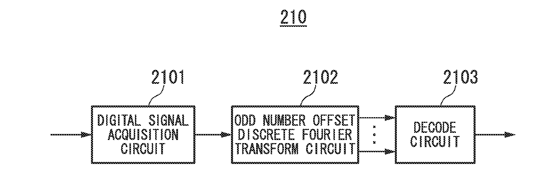
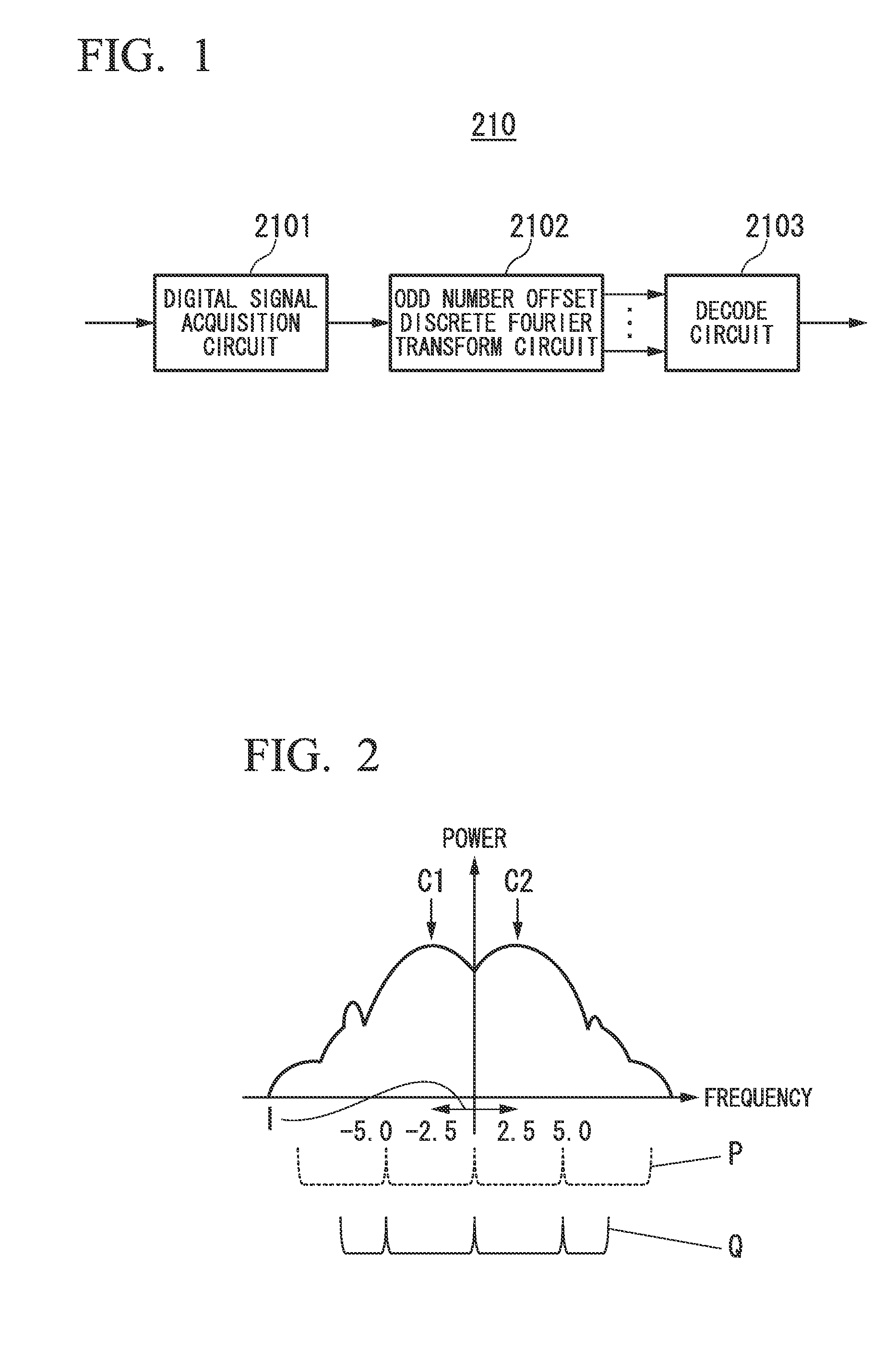
[0065]FIG. 1 is a block diagram showing the structure of a receiving device according to an embodiment B1 of the present invention.

[0066]A receiving device 210 shown in this figure includes a digital signal acquisition circuit 2101, an odd number offset discrete Fourier transform circuit 2102, and a decode circuit 2103.

[0067]The digital signal acquisition circuit 2101 converts received signals (analog signals) into digital signals.

[0068]The odd number offset discrete Fourier transform circuit 2102 applies an offset discrete Fourier transform, which is described later, to digital signals converted according to the received analog signals, and outputs frequency channels corresponding to the received signals. The decode circuit 2103 decodes the transmitted signals from the received signals of each of the frequency channels transformed by the odd number offset discrete Fourier transform circuit 2102.

[0069]Hereunder the specific operation of an offset discrete Fourier transform is descri...

embodiment b2

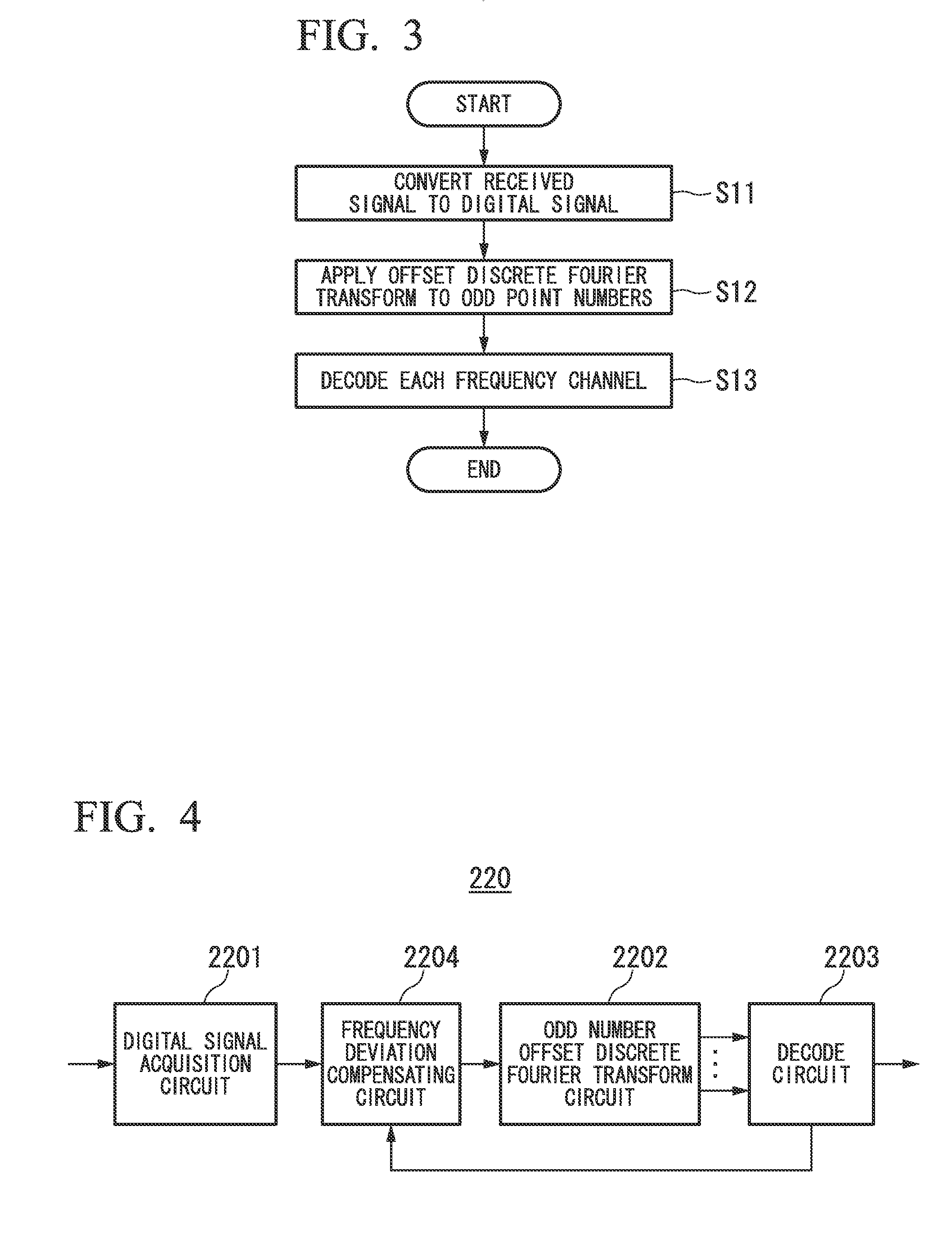
[0089]FIG. 4 is a block diagram showing the structure of a receiving device according to an embodiment B2 of the present invention.

[0090]A receiving device 220 shown in this figure includes a digital signal acquisition circuit 2201, an odd number offset discrete Fourier transform circuit 2202, a decode circuit 2203, and a frequency deviation compensating circuit 2204.

[0091]The digital signal acquisition circuit 2201 converts received signals (analog signals) into digital signals.

[0092]The frequency deviation compensating circuit 2204 compensates for frequency deviation occurring in the received signals using any of the received signals corresponding to the check signals inserted in the transmitted signals, the characteristics of the modulation system of the signals transmitted, and frequency deviation information input from other receiving circuit blocks. The frequency deviation occurring in the received signals denotes the frequency deviation between the frequency that generated th...

embodiment b3

[0106]FIG. 6 is a block diagram showing the structure of a receiving device according to an embodiment B3 of the present invention.

[0107]A receiving device 230 shown in this figure includes a digital signal acquisition circuit 2301, an odd number offset discrete Fourier transform circuit 2302, a decode circuit 2303, and a frequency deviation estimation circuit 2304.

[0108]The digital signal acquisition circuit 2301 converts received signals (analog signals) into digital signals. The frequency deviation estimation circuit 2304 compensates for frequency deviation occurring in the received signals using any of the received signals corresponding to the check signals inserted in the transmitted signals, the characteristics of the modulation system of the transmitted signals, and frequency deviation information input from other receiving circuit blocks. The frequency deviation occurring in the received signals denotes the frequency deviation between the frequency that generated the transmi...


PUM


Abstract

A frequency domain multiplexed signal receiving method which decodes received signals that are multiplexed in a frequency domain, includes: a digital signal acquisition step of acquiring digital signals from the received signals that are multiplexed in the frequency domain; an offset discrete Fourier transform step of applying an offset discrete Fourier transform to odd discrete point numbers based on the acquired digital signals; and a decode step of decoding frequency domain digital signals in the frequency domain obtained by the offset discrete Fourier transform, and that are the frequency domain digital signals of one or more frequency channels.

Description

TECHNICAL FIELD[0001]The present invention relates to a method for receiving frequency domain multiplexed signals and a device for receiving frequency domain multiplexed signals in a communication system in which signals are multiplexed in the frequency domain.[0002]Furthermore, the present invention relates to a method for receiving frequency domain multiplexed signals and a device for receiving frequency domain multiplexed signals in which received signals that have been multiplexed in the frequency domain are equalized without applying a discrete Fourier transform.[0003]Priority is claimed on Japanese Patent Application No. 2009-169460, filed Jul. 17, 2009, and Japanese Patent Application No. 2009-169455, filed Jul. 17, 2009, the contents of which are incorporated herein by reference.BACKGROUND ART[0004]In the field of wireless and optical communication, an orthogonal frequency division multiplexing system (OFDM: Orthogonal Frequency Division Multiplexing) is proposed for multipl...

Claims


Application Information

Patent Timeline
IPC IPC(8): H04L27/06H04L27/01
CPCH04L25/03159H04L27/2633H04L27/265H04L27/266H04L27/2672H04L2025/03414H04L27/26522
Inventor KUDO, RIICHIKOBAYASHI, TAKAYUKIISHIHARA, KOICHITAKATORI, YASUSHINOSAKA, HIDEYUKIMATSUI, MUNEHIROMIZOGUCHI, MASATONAKAGAWA, TADAOYAMAZAKI, ETSUSHISANO, AKIHIDEMIYAMOTO, YUTAKAYOSHIDA, EIJI
Owner NIPPON TELEGRAPH & TELEPHONE CORP
Learn More