Heat sinking element and method of treating a heat sinking element

a heat sinking element and heat sinking technology, applied in the field of heat sinking elements, can solve problems such as adversely affecting the reliability of chips, and achieve the effects of reducing the thermal resistance of the heat sinking element, improving the heat dissipation behaviour, and increasing the surface area

Active Publication Date: 2012-05-24
IND TECH RES INST
View PDF8 Cites 6 Cited by
  • Summary
  • Abstract
  • Description
  • Claims
  • Application Information

AI Technical Summary

Benefits of technology

[0010]A method of treating a heat sinking element is introduced herein to enhance the heat dissipation behaviour of the heat sinking element.
[0013]As embodied and broadly described herein, in an embodiment of the disclosure, an oxidation process and an etching process are performed on a surface of a metal substrate to form a heat sinking element. Therefore, the surface of the metal substrate has a plurality of micro-nano holes, thereby significantly increasing the surface area. In this manner, the thermal resistance of the heat sinking element is significantly lowered and the heat dissipation behaviour may be effectively improved. Therefore, the heat sinking element in an embodiment of the disclosure when applied in the heat dissipation design of an LED chip or other chips can provide an effective heat dissipation function.

Problems solved by technology

However, a thermal problem of the LED is still one of the major subjects in the development of the LED technique.
However, the EMI (Electromagnetic Interference) generated by the fan and the impact of vibration of the fan may adversely affect the reliability of the chip.

Method used


Image

  • Heat sinking element and method of treating a heat sinking element
  • Heat sinking element and method of treating a heat sinking element
  • Heat sinking element and method of treating a heat sinking element

Examples


Embodiment Construction

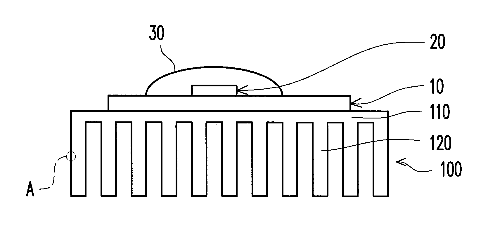
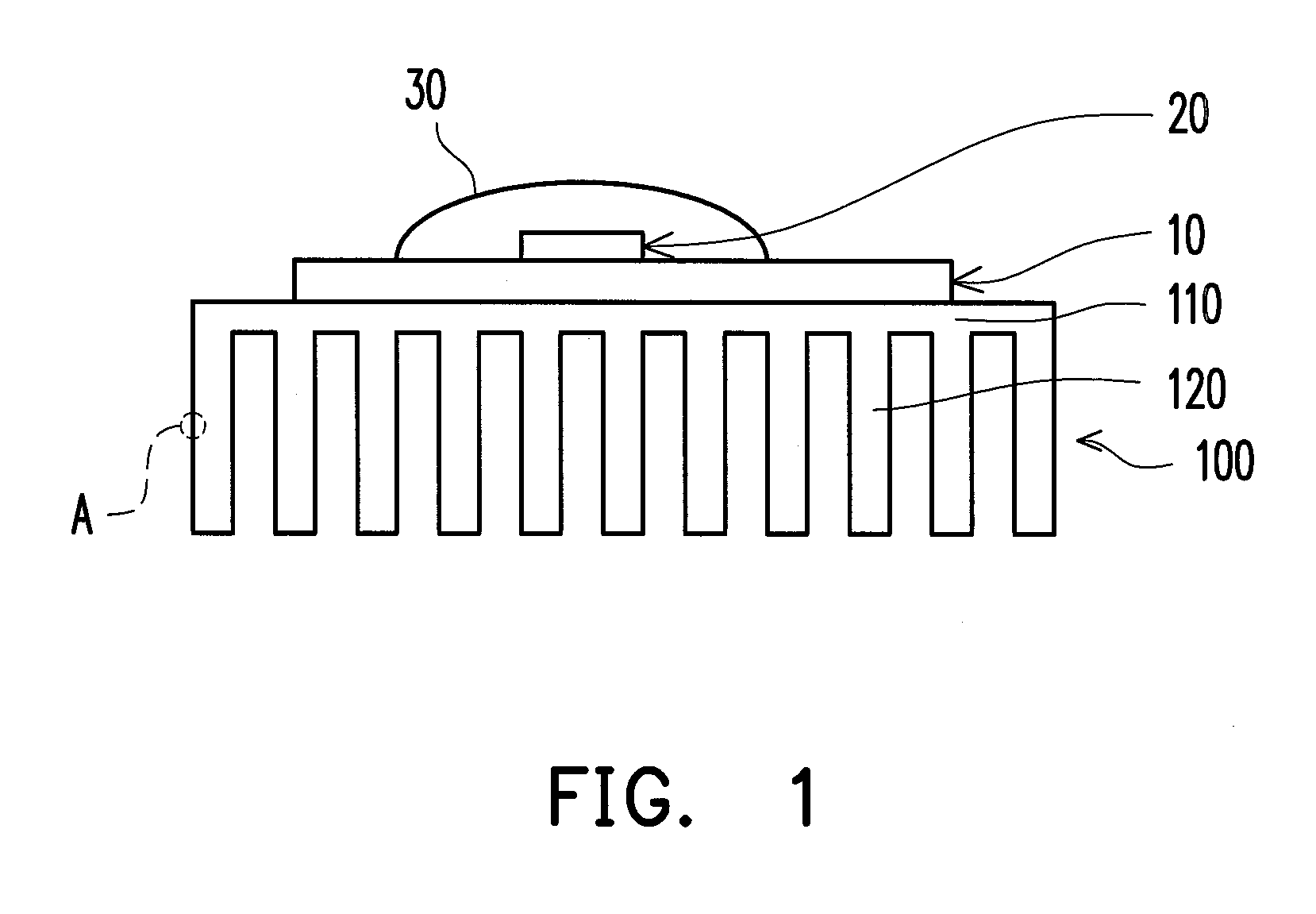
[0023]FIG. 1 illustrates a usage of a heat sinking element according to an embodiment of the disclosure. Referring to FIG. 1, a heat sinking element 100 is, for example, configured on one side of a substrate 10, and the other side of the substrate 10 is, for example, configured with a chip 20. The chip 20 is further covered by a polymer colloid 30. The chip 20 in FIG. 1 is, for example, an LED chip, but the disclosure is not limited to this and the chip 20 may also be other driving chip. In addition, the heat sinking element 100, for example, includes a seat 110 and a plurality of fins 120 connected to the seat 110, but in other embodiments of the disclosure, the heat sinking element 100 may also be a slug without the fins 120. That is, the heat sinking element 100 in FIG. 1 is only exemplary but not intended to limit the shape thereof.

[0024]The chip 20 and the heat sinking element 100 are respectively configured on two opposite sides of the substrate 10, so the heat sinking element...


PUM

PropertyMeasurementUnit
diameteraaaaaaaaaa
thicknessaaaaaaaaaa
thicknessaaaaaaaaaa

Abstract

A heat sinking element and a method of treating a heat sinking element are provided. The heat sinking element includes a metal substrate. The metal substrate is mainly composed of aluminium. A surface of the metal substrate has a plurality of micro-nano holes and a diameter of the micro-nano holes is smaller than 300 nm. The method of treating a heat sinking element includes performing an oxidation process and an etching process on the metal substrate so as to form the plurality of micro-nano holes.

Description

CROSS-REFERENCE TO RELATED APPLICATION[0001]This application claims the priority benefit of Taiwan application serial no. 99140576, filed on Nov. 24, 2010. The entirety of the above-mentioned patent application is hereby incorporated by reference herein and made a part of this specification.TECHNICAL FIELD[0002]The disclosure relates to a heat sinking element with a passive cooling design.BACKGROUND[0003]In recent years, due to the progressive development of the LED (Light Emitting Diode) semiconductor technique, the luminescence efficiency of chips has been greatly improved and the applications are found in all fields e.g. from a projector pen to illumination applications, and thus the application range has been greatly expanded. Furthermore, the LED has the advantages of small volume, long lifespan, low pollution, and low cost, has optical characteristics of good color saturation and dynamic color control and so on. Therefore, the LED based techniques attract more attentions.[0004...

Claims


Application Information

Patent Timeline
Patent Type & Authority Applications(United States)
IPC IPC(8): F28F13/18B05D3/10B82Y30/00B82Y40/00
CPCH01L23/367H01L33/642H01L2933/0075F21V29/89H01L2924/0002H01L2924/00Y10T428/249978
Inventor WANG, CHENG-CHUANYEN, CHIA-YINGCHEN, HSIN-HWA
Owner IND TECH RES INST
Why Eureka
Try Eureka