Layer structures for controlling stress of heteroepitaxially grown iii-nitride layers

a technology of iiinitride and heteroepitaxial growth, which is applied in the direction of basic electric elements, electrical equipment, semiconductor devices, etc., can solve the problems of iii-n epitaxial net tensile stress, cracking of the layers, and difficult to achieve thick iii-n layers on silicon substrates that are crack-free and exhibit adequate structural quality

Inactive Publication Date: 2012-05-24
TRANSPHORM INC
View PDF6 Cites 30 Cited by
  • Summary
  • Abstract
  • Description
  • Claims
  • Application Information

AI Technical Summary

Benefits of technology

[0008]For layer structures described above, one or more of the following may be applicable. The difference between the aluminum compositions of the at least two III-N well layers and the aluminum compositions of the at least two III-N barrier layers can be less than about 0.5 or less than about 0.2. The thickness of each of the III-N well layers can be between about 20 and 150 nm. The thickness of each of the III-N barrier layers can be less than about 100 Å or less than about 20 Å. The III-N barrier layers can have different thicknesses. The III-N barrier layers can have aluminum compositions between about 1 and 50 percent or between about 1 and 20 percent. The barrier layers can be AlGaN and the well layers can be GaN. The III-N well or barrier layers can be doped with a dopant selected from the group consisting of Fe, Mg, and B. The foreign substrate can be silicon. The foreign substrate can be selected from the group consisting of SiC, sapphire, and zinc oxide. The foreign substrate and the III-N layers each have thermal expansion coefficients, and the thermal expansion coefficient of the foreign substrate is can be smaller than the thermal expansion coefficient of one of the III-N layers. The second III-N structure can be atop the first III-N structure. The III-N buffer layer can be AlN. The additional III-N layer can be GaN or AlGaN. The additional III-N layer can be at least 2 microns thick or at least 5 microns thick. The additional III-N layer can be an epitaxial layer. Further layers atop the additional III-N layer can be included in the structure.
[0009]In another aspect, a III-N layer structure is described that includes a III-N buffer layer on a foreign substrate, an additional III-N layer, a first III-N structure, and a second III-N structure. The first III-N structure includes at least two AlxGayN layers where x+y is less than or equal to 1, and the layer of the two layers that is closer to the III-N buffer layer can have the larger aluminum composition. The second III-N structure includes a III-N superlattice, the III-N superlattice including at least two III-N well layers interleaved with at least two III-N barrier layers, the barrier layers each having an aluminum composition. The first III-N structure and the second III-N structure can be between the additional III-N layer and the foreign substrate. For the layer structures described above, one or more of the following may be applicable. Each of the AlxGayN layers can further include an element selected from the group consisting of Indium, Boron, Phosphorus, Arsenic, and Antimony. The difference between the aluminum compositions of the at least two III-N well layers and the aluminum compositions of the at least two III-N barrier layers can be less than about 0.5 or less than about 0.2. The thickness of each of the III-N well layers can be between about 20 and 150 nm. The thickness of each of the III-N barrier layers can be less than about 100 Å or less than about 20 Å. The III-N barrier layers can have different thicknesses. The III-N barrier layers can have aluminum compositions between about 1 and 50 percent or between about 1 and 20 percent. The III-N well or barrier layers can be doped with a dopant selected from the group consisting of Fe, Mg, and B. The barrier layers can be AlGaN and the well layers can be GaN.

Problems solved by technology

However, due to the large lattice mismatch and thermal expansion coefficient mismatch between silicon and III-N materials, there is typically a net tensile stress in III-N epitaxial layers deposited directly on silicon substrates.
This mismatch can result in cracking of the layers.
Therefore thick III-N layers on silicon substrates that are crack-free and that exhibit adequate structural quality can be difficult to achieve.
These deleterious effects may include defect formation and stress in the layers.
Therefore during cool down, the net tensile stress can cause cracking of the layer.
Hence, a sufficiently thick additional III-N layer, which may be necessary for many device applications, may not be possible with this prior art layer structure.
However, for the layer structure of FIG. 2, it has been shown that the maximum thickness of the additional III-N layer 12 that can be grown without the formation of substantial dislocations and other defects may be limited.
However, with these prior art layer structures, the maximum thickness of the additional epitaxial III-N layer 12 in FIGS. 1 and 2, that can be grown without sustaining substantial defects may be limited.
If these III-N epitaxial layers are grown too thick, tensile stress in the layer becomes substantial, which can cause cracking upon cooling.

Method used


Image

  • Layer structures for controlling stress of heteroepitaxially grown iii-nitride layers
  • Layer structures for controlling stress of heteroepitaxially grown iii-nitride layers
  • Layer structures for controlling stress of heteroepitaxially grown iii-nitride layers

Examples


Embodiment Construction

[0015]Devices formed by layer structures that include or are formed of III-N semiconductor layers, such as GaN and its alloys, grown atop foreign substrates, (i.e., substrates that differ substantially in composition and / or lattice structure from that of the deposited layers), such as silicon (Si), silicon carbide (SiC), or sapphire (Al2O3), are described herein. As used herein, the terms III-Nitride or III-N materials, layers or devices refer to a material or device comprised of a compound semiconductor material according to the stoichiometric formula AlxInyGazN, where x+y+z is about 1. Here, x, y, and z are compositions of Al, In and Ga, respectively.

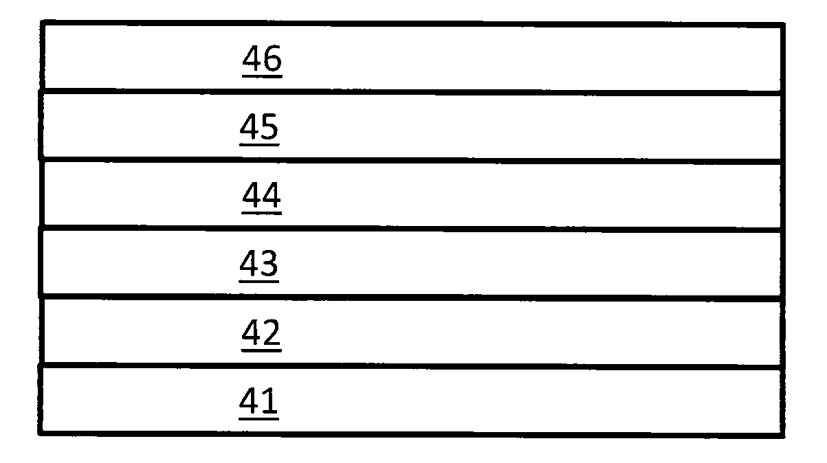
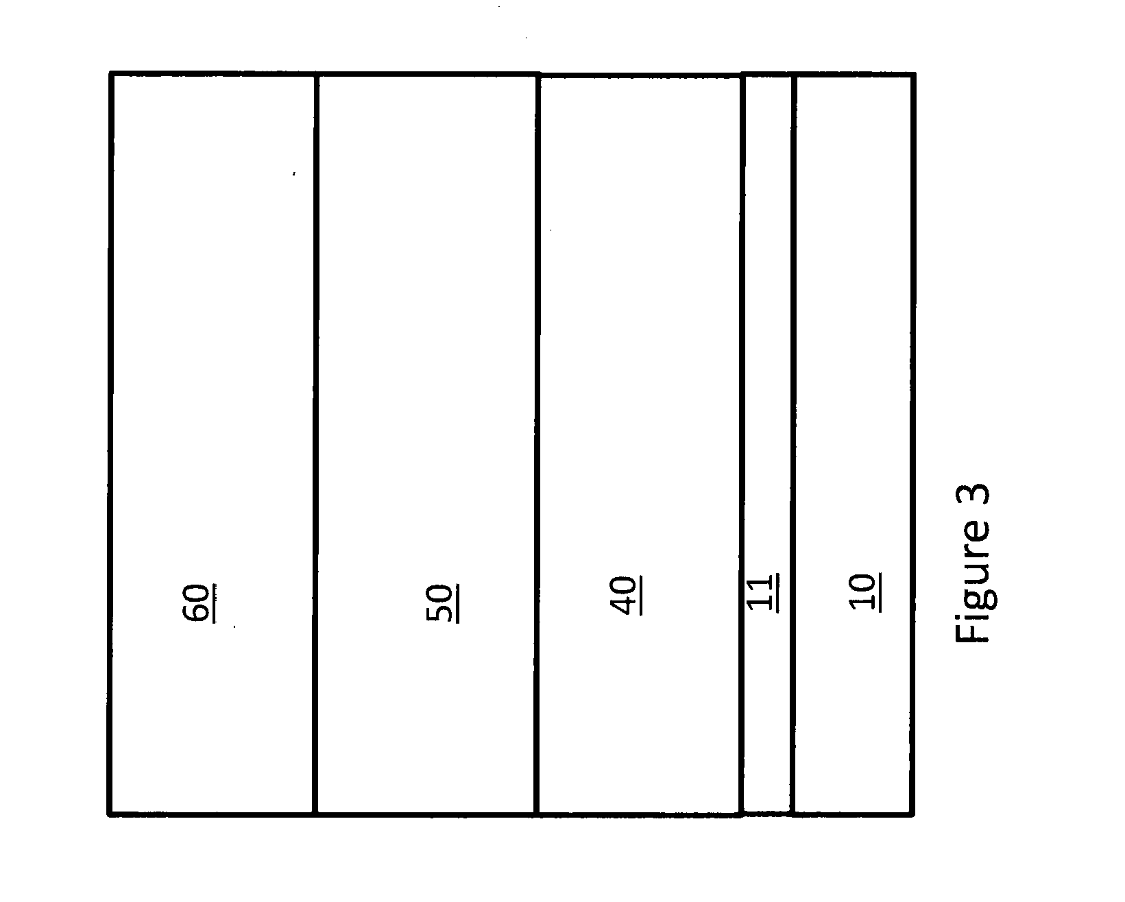
[0016]FIG. 3 shows a layer structure formed of layers of III-Nitride semiconductor materials on a foreign substrate 10, such as silicon. The layer structure includes silicon substrate 10, a III-N buffer layer 11, such as AlN, atop substrate 10, a first III-N structure 40 atop buffer layer 11, a second III-N structure 50 atop the first...


PUM


Abstract

A III-N layer structure is described that includes a III-N buffer layer on a foreign substrate, an additional III-N layer, a first III-N structure, and a second III-N layer structure. The first III-N structure atop the III-N buffer layer includes at least two III-N layers, each having an aluminum composition, and the III-N layer of the two III-N layers that is closer to the III-N buffer layer having the larger aluminum composition. The second III-N structure includes a III-N superlattice, the III-N superlattice including at least two III-N well layers interleaved with at least two III-N barrier layer. The first III-N structure and the second III-N structure are between the additional III-N layer and the foreign substrate.

Description

TECHNICAL FIELD[0001]This invention relates to growth of III-Nitride semiconductor films on silicon substrates, and specifically to methods to manage stress in the films.BACKGROUND[0002]As large native substrates for group III-Nitride (III-N) semiconductors are not yet widely available, III-N films, such as GaN and its alloys, are currently grown by heteroepitaxy on suitable non-III-N substrates. Typically, the films are grown on sapphire (Al2O3), silicon carbide (SiC), or silicon substrates. Silicon substrates are emerging as a particularly attractive substrate candidate for III-N layers due to their low cost, wide availability, large wafer sizes, thermal properties, and ease of integration with silicon-based electronics. However, due to the large lattice mismatch and thermal expansion coefficient mismatch between silicon and III-N materials, there is typically a net tensile stress in III-N epitaxial layers deposited directly on silicon substrates. This mismatch can result in crack...

Claims


Application Information

Patent Timeline
Patent Type & Authority Applications(United States)
IPC IPC(8): H01L29/20
CPCH01L21/0237H01L21/02458H01L29/7787H01L21/0254H01L29/2003H01L21/02507
Inventor KELLER, STACIAFICHTENBAUM, NICHOLAS
Owner TRANSPHORM INC
Why Eureka
Try Eureka