Stackable semiconductor chip with edge features and methods of fabricating and processing same

a technology edge features, which is applied in the field of stackable semiconductor chips with edge features and the method of fabricating and processing same, can solve problems such as becoming complicated or impossibl

Inactive Publication Date: 2012-05-31
ELECTRO SCI IND INC
View PDF8 Cites 28 Cited by
  • Summary
  • Abstract
  • Description
  • Claims
  • Application Information

AI Technical Summary

Benefits of technology

[0005]In accordance with this aspect of the invention, the function which is performed may consist of one or more testing, altering, repairing, programming, interrogating, loading and tuning as well as bonding one or more conductors into a functional relationship with a circuit or component on the chip.
[0006]Further in accordance with this first aspect of the invention, the edge feature may consist of one or more of an electrical conductor, a thermal conductor, a fuse, a resistor, a capacitor, an inductor, an optical emitter, an optical receiver, a test pad, a bond pad, a contact pin, a heat dissipation device, multiples of these and combinations of these.
[0007]Further in accordance with this first aspect of the invention, the signal conduit may consist of one or more of an electrical conductor such as a trace or a via, a heat conductor, an optical conductor, multiples of these and combinations of these.
[0008]Further in accordance with this first aspect of the invention, the method comprises the steps of locating the stack containing the semiconductor chip to be processed by way of an edge feature on a fixture wherein the edge feature can be addressed by a function performer and thereafter activating the function performer to address the edge feature. As used herein, a “chip” is a physical object with top and bottom primary surfaces, and one or more peripheral edge surface, the actual number of such edge surfaces being determined by chip geometry.
[0009]In accordance with

Problems solved by technology

This becomes complicated or impossible when the primary surfaces of the interior

Method used


Image

  • Stackable semiconductor chip with edge features and methods of fabricating and processing same
  • Stackable semiconductor chip with edge features and methods of fabricating and processing same
  • Stackable semiconductor chip with edge features and methods of fabricating and processing same

Examples


Embodiment Construction

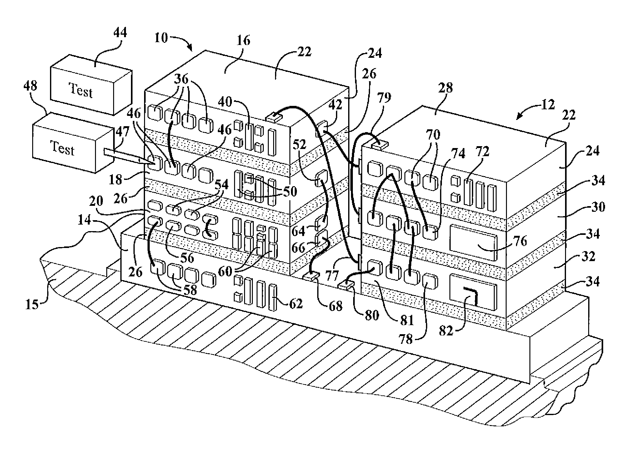
[0025]When semiconductor chips are bonded together in stacks, the primary surfaces of chips low in the stack are covered up. Therefore, access to features or devices on or associated with the primary surfaces is no longer possible for such functions as testing or wire bonding, or trimming or tuning or configuration change, redundancy, repair and / or encoding or programming. In accordance with the present invention, these and other functions are carried out by way of features which have been located in such a way as to be associated with one or more of the peripheral edge surfaces of the chips or dice. Thus, a die or chip which is fabricated in accordance with the present invention includes one or more edge features which facilitate or enable testing, wiring, repair, reconfiguration, tuning or processing despite the fact that the chip or die has been incorporated into a three-dimensional stack. Also disclosed herein are systems and devices to test, wire bond or otherwise process featu...


PUM


Abstract

A method of performing a function on a three-dimensional semiconductor chip package as well as on individual chips in the package is disclosed. That method involves the creation of an operative relationship between a function performer and an edge feature on the chip or chips wherein the edge feature consists of one or more of an electrically conductive pad, thermally conductive pad, a probe pad, a fuse, a resistor, a capacitor, an inductor, an optical emitter, an optical receiver, a test pad, a bond pad, a contact pin, a heat dissipator, an alignment marker, a metrology feature and a function performer may be any one or more of a test probe, the laser, a programming device, an interrogation device, a loading device or a tuning device. In addition, a chip per se with edge features is disclosed along with a three-dimensional stack of such chips in either of several different configurations. The disclosure provides information regarding the formation of edge feature, the singulation of dice having incipient edge features, the stacking of dice and the handling or dice with edge features.

Description

FIELD OF THE INVENTION[0001]This invention relates to semiconductor chips and more particularly to the fabrication and processing of a stackable semiconductor chip having edge features which facilitate or provide access to circuitry on or in the chip.BACKGROUND OF THE INVENTION[0002]Three-dimensional conductor chip packages comprising a stack of thin semiconductor chips are now being manufactured. The chips in these packages often contain controllers, memories, sensors, analog components, processors and specialty communications components as well as MEMS devices. The cost of these relatively dense, integrated packages is high, so quality control and testing as part of the fabrication, so quality control and testing as part of the fabrication process is all the more important.[0003]Functions such as testing, trimming, bonding and tuning are typically carried out by accessing the primary surfaces of the semiconductor chips, usually a planar top surface. The accessing step may require ...

Claims


Application Information

Patent Timeline
IPC IPC(8): H01L21/66H01L23/48G01R1/06
CPCG01R31/2884H01L22/32H01L2924/1461H01L2224/48091H01L2924/3011H01L25/0652H01L25/0657H01L2225/06506H01L2225/0651H01L2225/06534H01L2225/06551H01L2225/06596H01L2924/00014H01L2924/00H01L25/00H01L23/58G01R31/26
Inventor BRULAND, KELLYWEBB, TIMOTHY R.HOOPER, ANDY E.CARRUTHERS, JOHN R.
Owner ELECTRO SCI IND INC
Why Eureka
Try Eureka