
Driver element and display device

Inactive Publication Date: 2012-05-31
KYOCERA CORP
View PDF1 Cites 19 Cited by
  • Summary
  • Abstract
  • Description
  • Claims
  • Application Information

AI Technical Summary

Benefits of technology

[0011]Therefore, it is an object of the present invention to provide a driver element and a display device whereby it is possible to further reduce the distance between the driving IC and the display portion.
[0017]According to the present invention, it is possible to broaden a substantial area for wiring between the display portion and the driver element, and it is possible to further reduce the distance between the driver element and the display portion. Further, it is possible to increase the number of wirings between the driver element and the display portion.

Problems solved by technology

However, if the driving IC is mounted close to the display portion, the wiring region becomes small, and it tends to be difficult to provide a wiring pattern.
That is, it is difficult to reduce the distance between the driving IC and the display portion beyond a certain level in order for the wiring pattern to be provided.

Method used


Image

  • Driver element and display device
  • Driver element and display device
  • Driver element and display device

Examples


embodiment 1

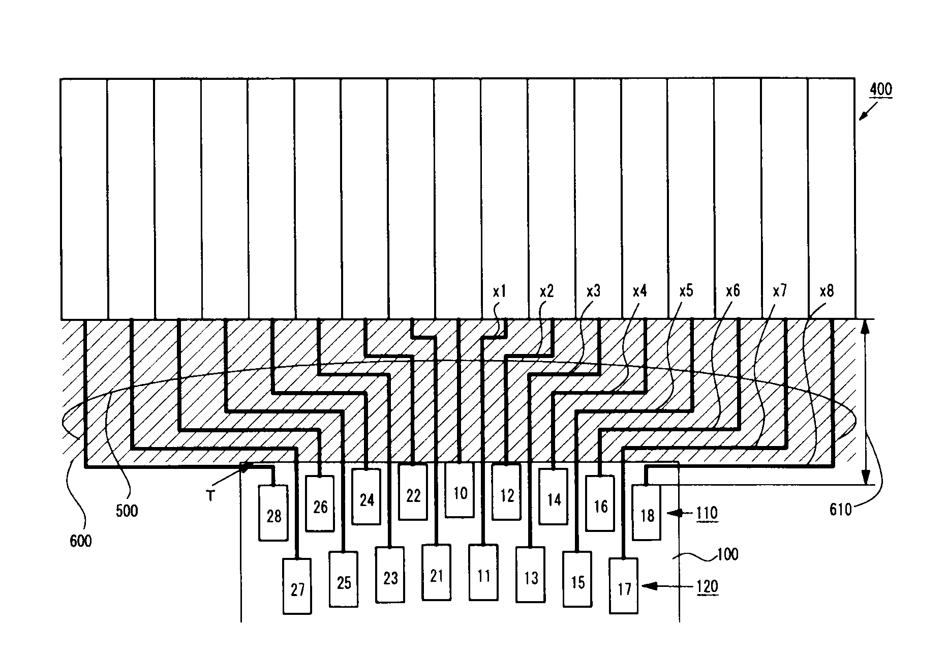
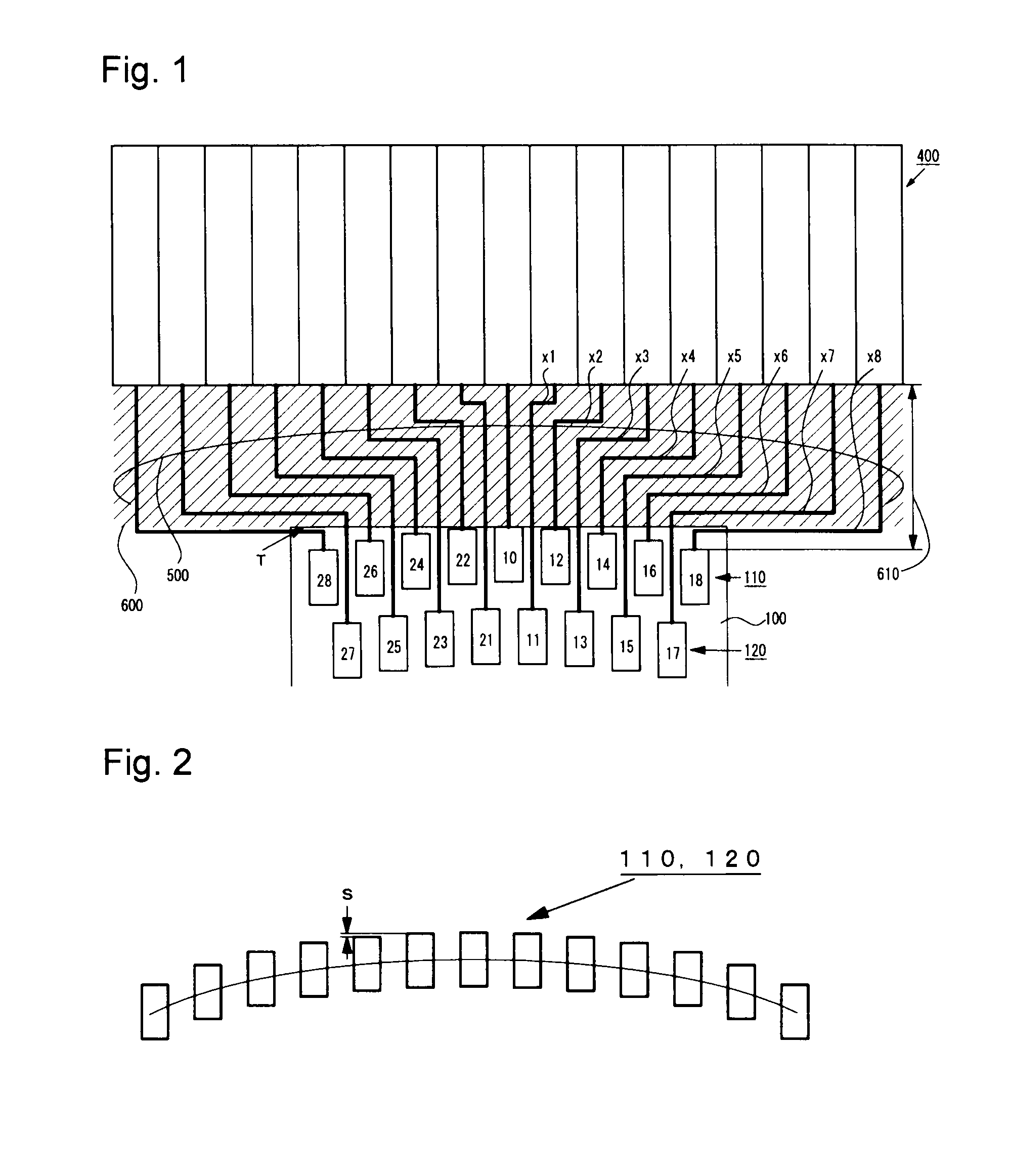
[0027]FIG. 1 is a block diagram illustrating a driving IC (driver element) 100 according to the present invention together with a display portion 400 to be driven by driving signals output from the driving IC 100 and a wiring pattern 500 in a wiring region 600. In this embodiment, the display portion 400 is a liquid crystal display portion employing TFT (Thin Film Transistor), and the driving IC 100 is a source driver to drive source electrodes in the liquid display portion. Further, the wiring pattern 500 includes wirings to connect the respective source wirings and electrode pads connected to the respective bumps.

[0028]In the example shown in FIG. 1, each wiring in the wiring pattern 500 is disposed linearly or as bent at 90°, between an electrode pad and a source wiring.

[0029]Here, in FIG. 1, vertically long rectangles in the display portion 400 correspond, respectively, to pixel columns connected to source wirings of the respective columns. Further, in the driving IC 100, bumps ...


PUM


Abstract

To broaden a substantial area for wiring between a display portion and a driver element, and to increase the number of wirings between the driver element and the display portion.In a driving IC 100, bumps 10, 12, 14, 16, 18, 22, 24, 26 and 28 are arrayed in a first row 110 and bumps 11, 13, 15, 17, 21, 23, 25, 27 are arrayed in a second row 120, wherein the respective bumps are disposed so that the shortest distances between forward ends of the respective bumps and a side along the array, become larger gradually from the center outward in the array.

Description

BACKGROUND OF THE INVENTION[0001]1. Field of the Invention[0002]The present invention relates to a driver element to be mounted on a display device such as a liquid crystal display device, and a display device having the driver element mounted thereon.[0003]2. Discussion of Background[0004]A liquid crystal display device or an organic EL (Electro Luminescence) display device is provided with a display portion in a display panel and a driver element (hereinafter referred to as a driving IC) to supply driving signals to the display portion.[0005]As a system to connect the display portion and the driving IC, a COG (Chip On Glass) system is widely used. In the COG system, a method is commonly used wherein bumps (bump electrodes) formed on a mounting surface i.e. a surface on the side to be mounted on a glass substrate in the driving IC, are connected to electrode pads formed on the glass substrate, via a conductive material such as an anisotropically conductive film.[0006]As shown in FI...

Claims


Application Information

Patent Timeline
IPC IPC(8): H05K7/00H05K1/00
CPCH05K1/0306H05K1/111G02F1/13452H05K2201/10128H05K2201/09418
Inventor GONDO, KENJI
Owner KYOCERA CORP
Features
  • Generate Ideas
  • Intellectual Property
  • Life Sciences
  • Materials
  • Tech Scout
  • Unparalleled Data Quality
  • Higher Quality Content
  • 60% Fewer Hallucinations
Learn More