Dual gate electronic memory cell and device with dual gate electronic memory cells

a technology of electronic memory cells and electronic memory cells, which is applied in the field of dual gate electronic memory devices, can solve the problems of reducing the reliability of memory, reducing the thickness of the tunnel oxide of the memory, and restricting the reduction of the size of the memory,

Inactive Publication Date: 2012-06-07
COMMISSARIAT A LENERGIE ATOMIQUE ET AUX ENERGIES ALTERNATIVES
View PDF1 Cites 14 Cited by
  • Summary
  • Abstract
  • Description
  • Claims
  • Application Information

AI Technical Summary

Benefits of technology

[0017]Thus there is a need to provide a new dual gate electronic memory cell enabling to make an electrical recontacting of each gate without any risk of short circuit between the gates, which does not require a very accurate alignment of electrical contacts with respect to the gates of the memory cells, and this without having to implement a further photolithography level dedicated to this electrical recontacting.
[0027]Because the electrical contact pad made as two lateral spacers is formed from the same materials forming the second gate, this electrical contact pad can thus be made without requiring implementing a photolithography step dedicated to the making thereof.

Problems solved by technology

However, such memories have drawbacks restricting the reduction of their sizes.
On the other hand, sustained use of such a memory (repeated writing-erasing cycles) generates defects in the tunnel oxide which will assist charge conduction and degrade charge retention in the floating gate, which is an issue in the case of a high SILC.
In practice, it is thus difficult to reduce the thickness of the tunnel oxide of these memories to less than 8 nm without SILC becoming a critical phenomenon for storage.
Moreover, by reducing the dimensions of such a memory cell, cross-coupling between floating gates of two adjacent cells of a same memory becomes significant and can thus degrade the memory reliability.
One of the difficulties for making these memories resides in controlling the position of gates (control gate and storage gate) with respect to one another.
A bad control of the relative positions of both gates thus results in a bad control in the electrical characteristics of the second transistor, and thus a bad performance of the memory.
However, with such a structure, it is very difficult to perform afterwards an electrical recontacting on the storage gate in view of the low dimensions of this gate as a natural spacer.
Furthermore, because of the proximity of the storage gate with the control gate, there is a very high risk that the electrical contact made on the gate as a spacer creates a short circuit between both gates in case of misalignment upon making the electrical contact.

Method used


Image

  • Dual gate electronic memory cell and device with dual gate electronic memory cells
  • Dual gate electronic memory cell and device with dual gate electronic memory cells
  • Dual gate electronic memory cell and device with dual gate electronic memory cells

Examples


first embodiment

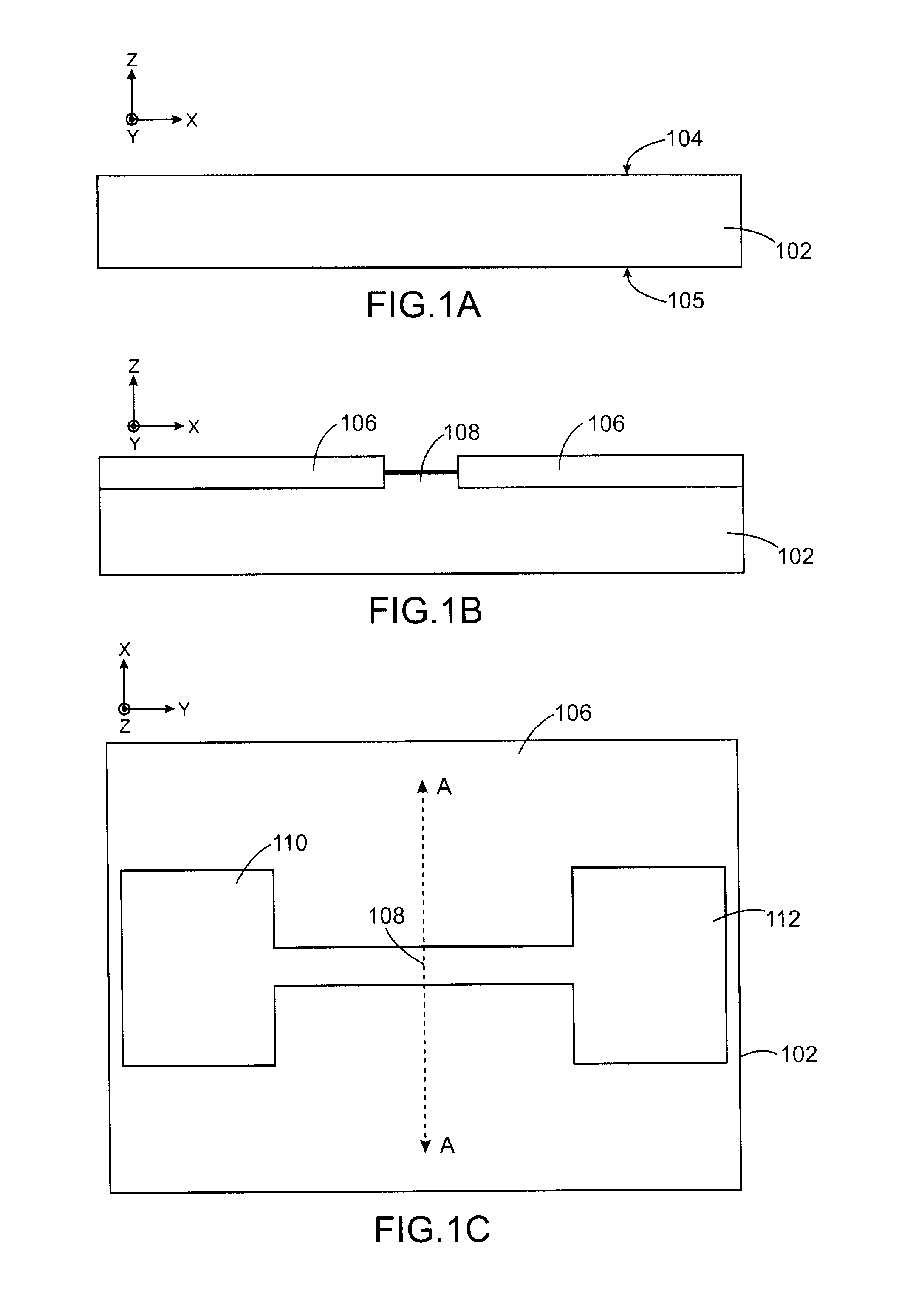
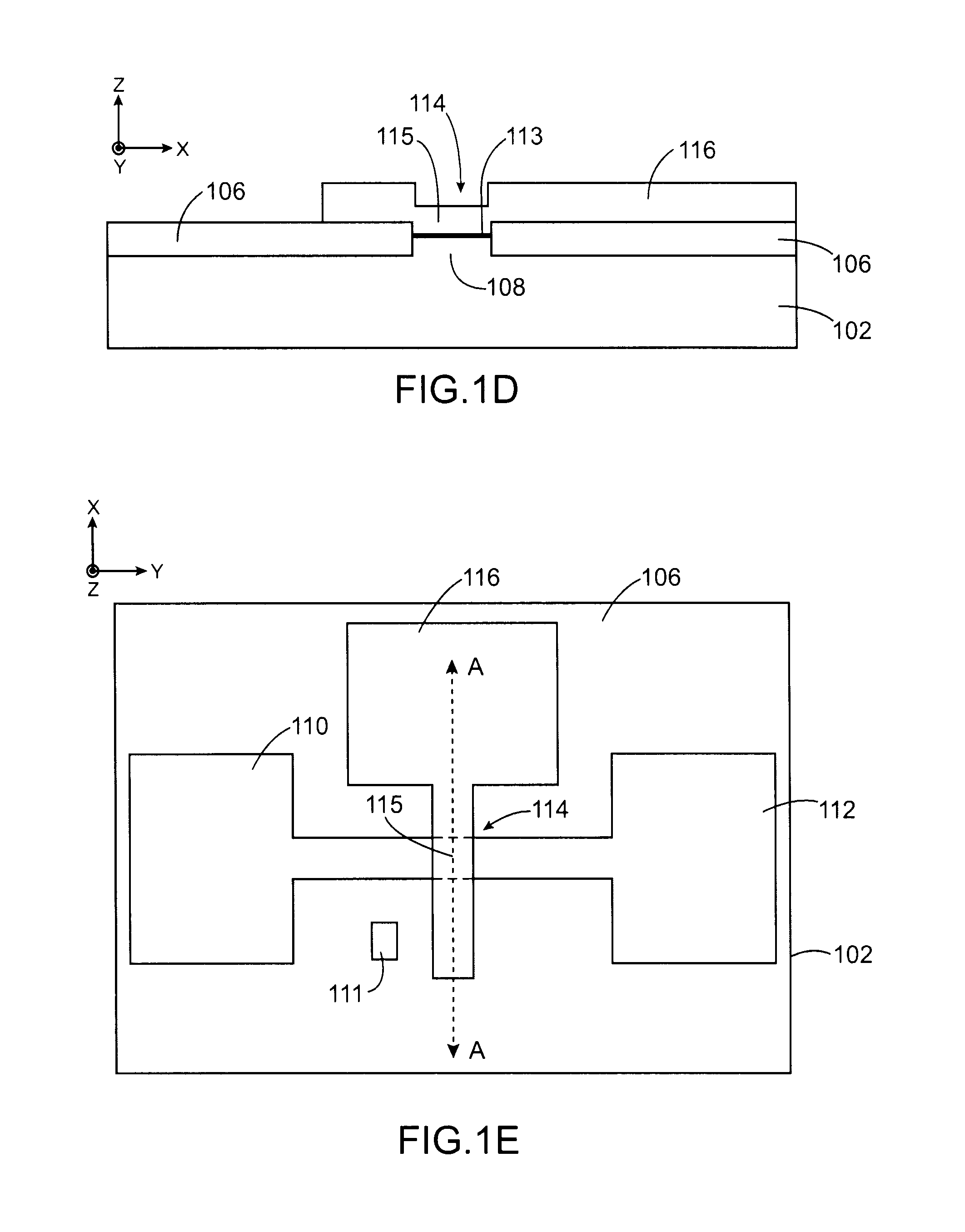
[0057]FIGS. 1A to 1O represent steps of a method for making a memory cell

second embodiment

[0058]FIGS. 2A to 2C represent a memory cell

[0059]FIGS. 3, 4A and 4B represent a memory cell according to alternatives of the first and second embodiments,

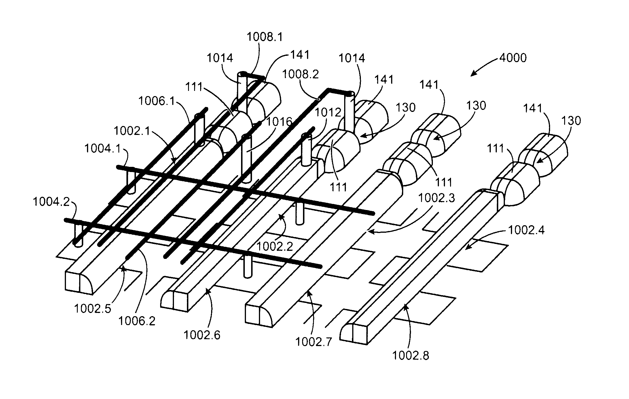
[0060]FIGS. 5 to 12B represent memory devices made according to different alternative embodiments.

[0061]Identical, similar or equivalent parts of the different figures described hereafter have the same reference numerals so as to make it easier to switch from one figure to the other.

[0062]Different parts represented on the figures are not drawn necessarily to an uniform scale, for the figures to be more intelligible.

[0063]Different possibilities (alternatives and embodiments) should be understood as being not exclusive from each other and can be combined between each other.


PUM


Abstract

A memory cell including:an active area having a channel provided between a source and a drain,a first gate provided on a first part of the channel,a portion of a first lateral spacer provided against a lateral flank of the first gate, a part of which forms a second gate provided on a second part of the channel,one of two gates forming a storing gate,the memory cell further including a portion of a second lateral spacer provided against a lateral flank of a block provided on the semi-conductor layer, the second lateral spacer being in contact with the first lateral spacer, the first and second lateral spacers being composed of similar materials, said portion of the second lateral spacer forming a part of an electrical contact pad electrically connected to the second gate.

Description

TECHNICAL FIELD[0001]This invention relates to the field of non-volatile electronic memory devices, or memories, and more particularly the field of dual gate (floating gate for storage and control gate) Flash type electronic memories.STATE OF PRIOR ART[0002]There are several types of non-volatile memories, that is memories preserving stored information in the absence of power supply, that can be electrically written and / or erased:[0003]EPROMs (“Erasable Programmable Read Only Memories”), the content of which can be electrically written, but which can be subjected to UV radiation to erase the stored information,[0004]EEPROMs (“Electrically Erasable Programmable ROMs”) the content of which can be electrically written and erased, but which require, for manufacture thereof, higher semi-conductor areas than EPROM type memories, and which thus are more costly to make.[0005]There are also non-volatile memories, called Flash memories, which do not have the drawbacks of the abovementioned EP...

Claims


Application Information

Patent Timeline
Patent Type & Authority Applications(United States)
IPC IPC(8): H01L29/788H01L21/336
CPCG11C16/0433H01L21/28282H01L29/792H01L29/42344H01L27/11568H01L29/40117H10B43/30
Inventor GELY, MARCMOLAS, GABRIEL
Owner COMMISSARIAT A LENERGIE ATOMIQUE ET AUX ENERGIES ALTERNATIVES
Why Eureka
Try Eureka