Method for manufacturing semiconductor device

a manufacturing method and semiconductor technology, applied in semiconductor devices, semiconductor/solid-state device details, electrical devices, etc., can solve the problems of difficult control of body voltage, difficult to control body voltage, and short channel effect of semiconductor devices, so as to reduce short channel effect, avoid short circuit of adjacent transistors, and reduce the dimension of semiconductor devices.

Inactive Publication Date: 2015-04-09
NAN YA TECH
View PDF5 Cites 2 Cited by
  • Summary
  • Abstract
  • Description
  • Claims
  • Application Information

AI Technical Summary

Benefits of technology

[0006]The present disclosure is to provide a semiconductor device and a method for fabricating the same, which reduce the short channel effect while the dimension of the transistor of the semiconductor device is reduced. Furthermore, the risk of short circuit of adjacent transistors is also avoided.

Problems solved by technology

However, as a semiconductor device is shrunk, characteristics of the transistor of the semiconductor device are degraded by a short channel effect.
To solve this issue, on one hand, various structures of planar transistor have been suggested to extend the channel length; however, there are still various concerns to limit it from manufacturing.
A vertical transistor has doped source and drain regions, which are formed in a vertical direction, and thus a channel region is vertically formed in a substrate; however, it is difficult to control a body voltage in the vertical transistor having a channel region formed of an undoped silicon (Si) in the related art.
Therefore, the vertical transistor has a difficulty in effectively controlling phenomena such as a punch-through effect or a floating body effect.
That is, while the vertical transistor is not in operation, a gate induced drain leakage (GIDL) effect is caused due to holes accumulated in a body.
Thereby, a current loss in the transistor frequently occurs and charges stored in a capacitor are drained so that a loss of original data is caused.

Method used


Image

  • Method for manufacturing semiconductor device
  • Method for manufacturing semiconductor device
  • Method for manufacturing semiconductor device

Examples


Embodiment Construction

[0033]The present disclosure is described by the following specific embodiments. Those with ordinary skill in the arts can readily understand the other advantages and functions of the present disclosure after reading the disclosure of this specification. The present disclosure can also be implemented with different embodiments. Various details described in this specification can be modified based on different viewpoints and applications without departing from the scope of the present disclosure.

[0034]As used herein, the singular forms “a,”“an” and “the” include plural referents unless the context clearly dictates otherwise. Therefore, reference to, for example, a data sequence includes aspects having two or more such sequences, unless the context clearly indicates otherwise.

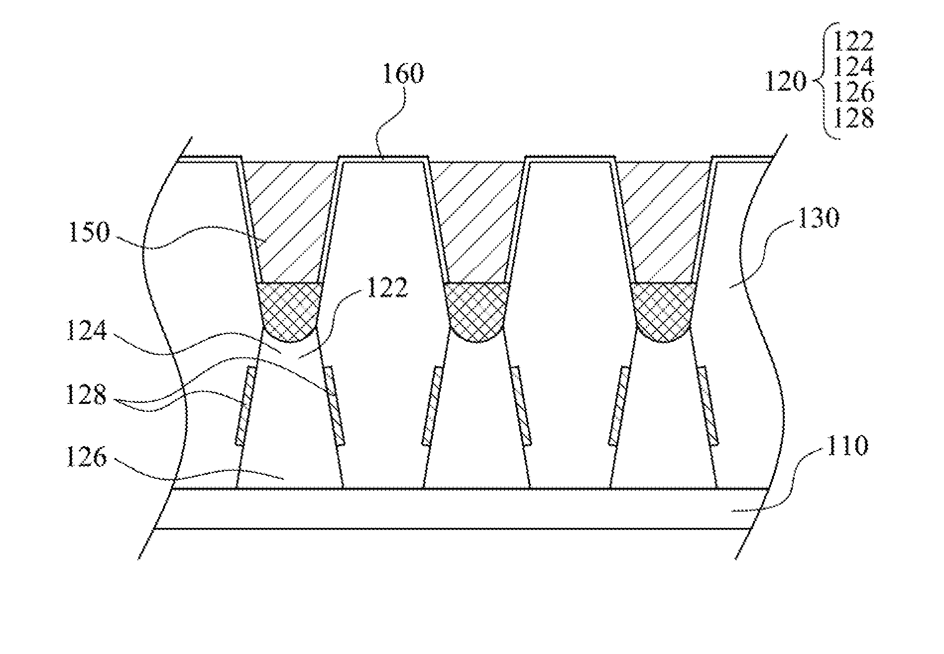
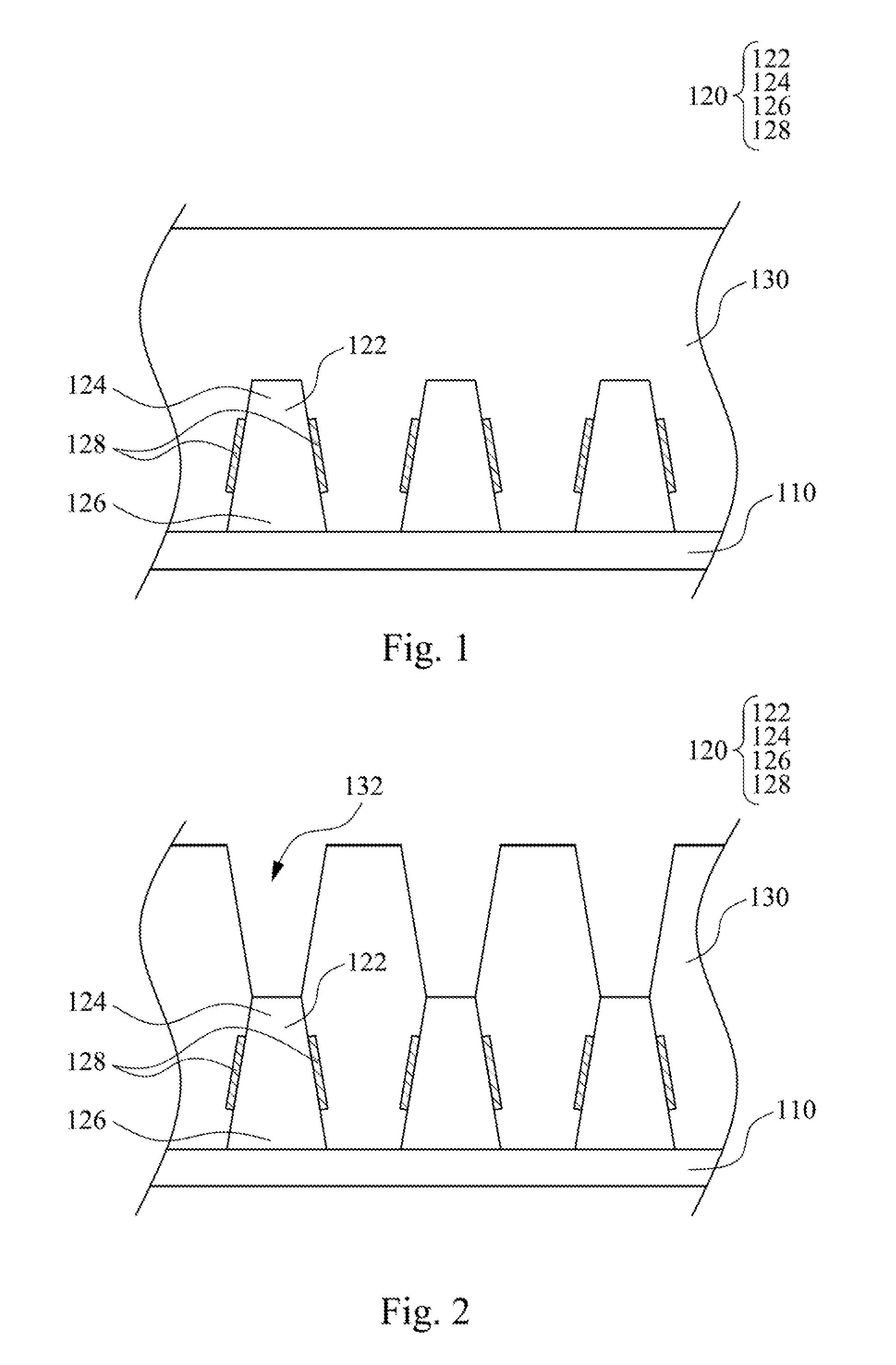
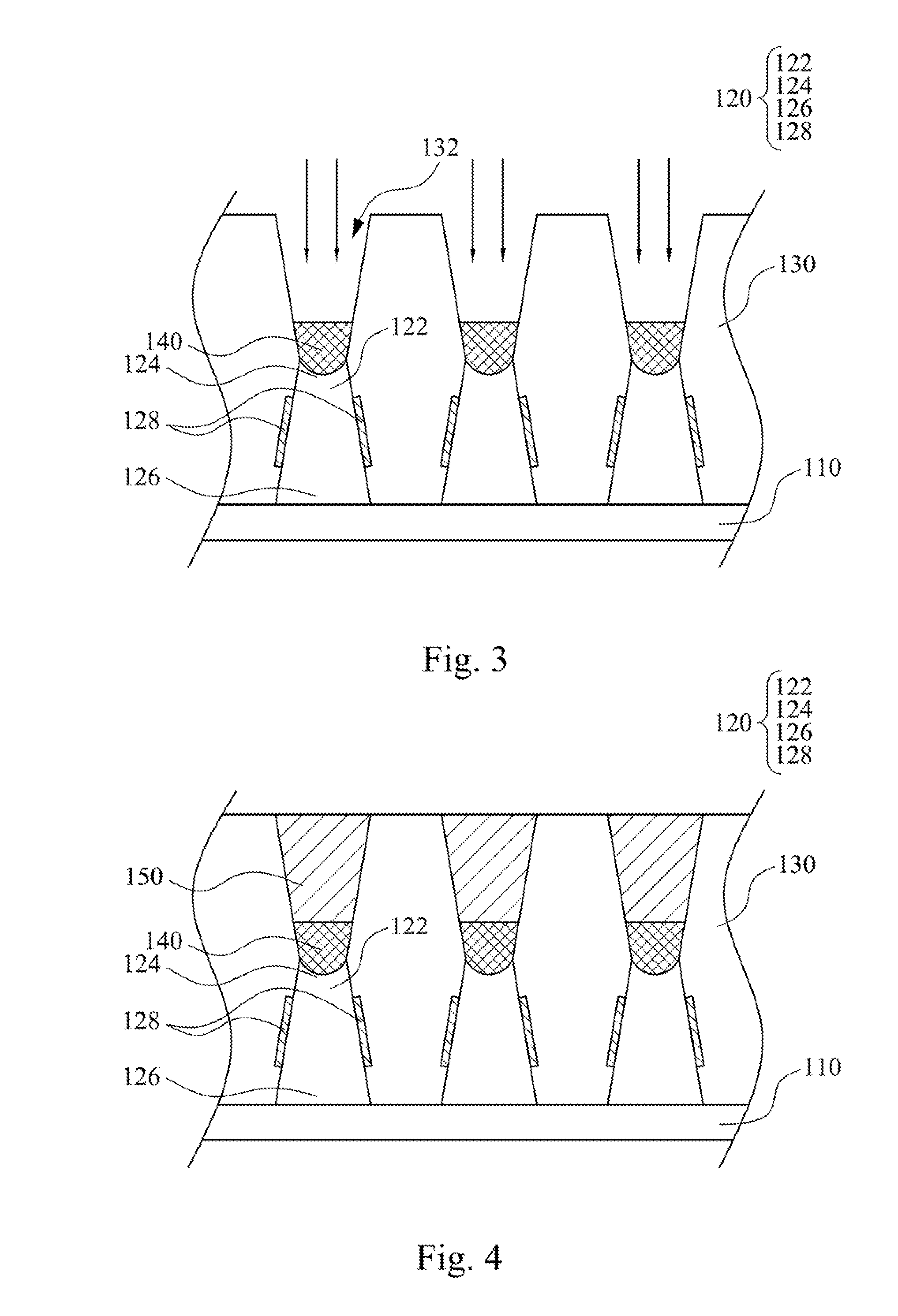
[0035]Reference will now be made in detail to the embodiments of the present disclosure, examples of which are illustrated in the accompanying drawings. Wherever possible, the same reference numbers are used in t...


PUM


Abstract

Provided is a method for fabricating a semiconductor device, which includes the following steps. First, a substrate having at least one transistor is provided. A first insulation layer is formed to cover the transistor. The first insulation layer is patterned to form at least one opening, wherein a part of the transistor is exposed by the opening. At last, an epitaxy is formed in the opening to cover the part of the transistor.

Description

BACKGROUND[0001]1. Technical Field[0002]The present invention relates to a method for manufacturing an electronic device, more particularly, to a method for manufacturing a semiconductor device.[0003]2. Description of Related Art[0004]Among semiconductor memory devices, dynamic random access memories (DRAMs) have been widely used. Generally, each cell of a DRAM has a MOS transistor which enables data charges in the storage capacitor to move in data read and write operations.[0005]To be highly integrated, the DRAM should have a capacitor with a sufficient storage capacity and a small unit cell size. In particular, a general approach to reduce a production cost of DRAM is to increase an integration level. To improve an integration density of the DRAM cell, a unit cell size of the DRAM cell needs to be reduced. However, as a semiconductor device is shrunk, characteristics of the transistor of the semiconductor device are degraded by a short channel effect. To solve this issue, on one h...

Claims


Application Information

Patent Timeline
Patent Type & Authority Applications(United States)
IPC IPC(8): H01L29/78H01L23/48H01L21/768H01L29/66
CPCH01L29/7827H01L21/76879H01L23/481H01L29/66666H01L21/28525H01L29/0847H01L29/41783H01L29/66628H01L29/0657H01L2924/0002H10B12/34H10B12/053H01L2924/00H01L29/42392H10B12/05H10B12/30H01L21/28562H01L29/456H01L29/66568
Inventor CHI, HUNG-YUYU, CHIEN-ANLIN, YI-FONGCHEN, FENG-LING
Owner NAN YA TECH
Why Eureka
Try Eureka