

Aqueous composition for etching of copper and copper alloys
a technology of etching composition and copper alloy, which is applied in the field of etching composition of copper and copper alloy, can solve the problems of inability to use conventional etching solutions, disadvantages of known etching solutions, and on-going miniaturization of circuits in terms of line width, value and thickness of copper layers to be etched, so as to minimize the risk of circuit shorts between individual copper or copper alloy structures
Inactive Publication Date: 2014-09-18
ATOTECH DEUT GMBH
View PDF3 Cites 1 Cited by
- Summary
- Abstract
- Description
- Claims
- Application Information
AI Technical Summary
Benefits of technology
The present invention provides an aqueous composition that can create a rectangular line shape when etched copper or copper alloy structures are applied. This reduces the risk of circuit shorts between copper structures and ensures sufficient adhesion between the copper structures and the underlying dielectric substrate.
Problems solved by technology
The ongoing miniaturization of circuits in terms of line width / interline-space values and thickness of the copper layers to be etched does not allow to use conventional etching solutions such as the ones described above.
The disadvantage of known etching solutions is even more present if the copper tracks are manufactured by a semi additive process (SAP).
Etching solutions based on sulfuric acid and hydrogen peroxide lead to an undesired undercutting of the first copper layer during etching (FIG. 1) which results in an insufficient adhesion of the copper layer on the dielectric substrate.
The broader base of the etched copper line can lead to circuit shorts which are not acceptable.
Method used
View moreImage
Smart ImageViewing Examples


Examples
example 3
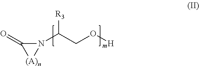
[0056]An aqueous composition consisting of 15 g / l Fe2(SO4)3, 90 g / l sulfuric acid and 0.1 g / l of a N-ethoxylated Polyamide 6, obtained by a ring-opening polymerization of ∈-caprolactam-N-ethoxylate was applied as etching solution.
[0057]The resulting line shape of the copper tracks (track width: 8 μm, track height: 10 μm) is shown in FIG. 3. The copper tracks have the desired rectangular line shape, have a sufficient adhesion to the underlying dielectric substrate and pose no risk for circuit shorts.
Login to View More PUM
| Property | Measurement | Unit |
|---|---|---|
| temperature | aaaaa | aaaaa |
| temperature | aaaaa | aaaaa |
| concentration | aaaaa | aaaaa |
Abstract
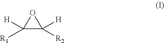
The present invention relates to an aqueous composition and a process for etching of copper and copper alloys. The aqueous composition comprises Fe3+ ions, an acid and a N-alkoxylated polyamide. The aqueous composition is particularly useful for making of fine structures in the manufacture of printed circuit boards, IC substrates and the like.
Description
FIELD OF THE INVENTION[0001]The invention relates to aqueous compositions for etching of copper and copper alloys and a process for etching of copper and copper alloys in the manufacture of printed circuit boards, IC substrates, copperised semiconductor wafers and the like.BACKGROUND OF THE INVENTION[0002]Circuit formation by etching of copper or copper alloy layers is a standard manufacturing step in production of printed circuit boards, IC substrates and related devices.[0003]A negative pattern of the circuit is formed by a) applying an etch resist, e.g., a polymeric dry film resist or a metal resist on a layer of copper, b) etching away those portions of copper not covered by the etch resist and c) remove the etch resist from the remaining copper circuit.[0004]Etching solutions applied for this task are selected from different types of compositions such as mixtures of an oxidizing agent and an acid. Two main types of etching solutions are based on an acid such as sulphuric acid o...
Claims
Login to View More Application Information
Patent Timeline
 Patent Type & AuthorityApplications(United States)
IPC IPC(8): C23F1/18C25D5/34
CPCC23F1/18C23F1/44C23F1/46C25D5/34H05K3/067H05K3/108H05K2203/0789H01L21/32134
InventorLÜTZOW, NORBERTTHOMS, MARTINEXNER, ANIKAKLOPPISCH, MIRKO
OwnerATOTECH DEUT GMBH