Electro-optical device with undercut-reducing thin film pattern and reticle

a thin film pattern and electronic device technology, applied in optics, originals for photomechanical treatment, instruments, etc., can solve the problems of inability to accurately operate the thin film semiconductor device, the subject of related art photolithographic technology, and the risk of short circuit between the thin film and the other thin film is high, and the risk of occurrence of undercut is reduced. , the effect of small thickness

Inactive Publication Date: 2005-01-04
BOE TECH GRP CO LTD
View PDF7 Cites 2 Cited by
  • Summary
  • Abstract
  • Description
  • Claims
  • Application Information

AI Technical Summary

Benefits of technology

With this variation, an advantage of the present invention can be more effectively obtained. That is, in this variation, the other thin film composed of a conductive material is formed on the thin film with the insulating film interposed therebetween, the insulating film having a relatively small thickness in the range from 10 to 150 nm. As a result, the risk of short circuiting between the thin film and the other thin film would be high if the above-mentioned undercut is produced; however, in this variation, since the “smooth intersection” is formed, the risk of occurrence of the undercut is reduced, thereby reducing the risk of the short circuiting.
can be more effectively obtained. That is, in this variation, the other thin film composed of a conductive material is formed on the thin film with the insulating film interposed therebetween, the insulating film having a relatively small thickness in the range from 10 to 150 nm. As a result, the risk of short circuiting between the thin film and the other thin film would be high if the above-mentioned undercut is produced; however, in this variation, since the “smooth intersection” is formed, the risk of occurrence of the undercut is reduced, thereby reducing the risk of the short circuiting.
Accordingly, with this variation, an accurate operation of the thin film semiconductor device can be achieved.
In another variation of the fourth thin-film semiconductor device, each of the angles formed between the additional line segment and the one line segment and between the additional line segment and the other line segment is about 135°.
With this variation, the “additional line segment” is assumed to lie between the one line segment and the other line segment, which would be, for example, orthogonal to each other without the additional line segment, so as to obliquely bridge ends of these two line segments. This is one of the variations in which a “smooth” connection between the one line segment and the other line segment is most effectively achieved without making the pattern complicated.
In another variation of the fourth thin-film semiconductor device, an insulating film having a thickness equal to or less than 50 nm is formed on the thin film and another thin film comprising a conductive material is formed on the insulating film, and each of the angles formed between the additional line segment and the one line segment and between the additional line segment and the other line segment is greater than 135°.

Problems solved by technology

However, the related art photolithographic technology is subject to the following problems.
This state alone is a problem from the viewpoint of stability of a thin-film semiconductor device.
It is believed that this causes a short circuit between the patterned film and the film composed of a conductive material.
In this state, for example, even when it is intended to activate only the patterned film, the film composed of a conductive material is also activated at the same time, and therefore an accurate operation of the thin-film semiconductor device cannot be expected.

Method used


Image

  • Electro-optical device with undercut-reducing thin film pattern and reticle
  • Electro-optical device with undercut-reducing thin film pattern and reticle
  • Electro-optical device with undercut-reducing thin film pattern and reticle

Examples


first exemplary embodiment

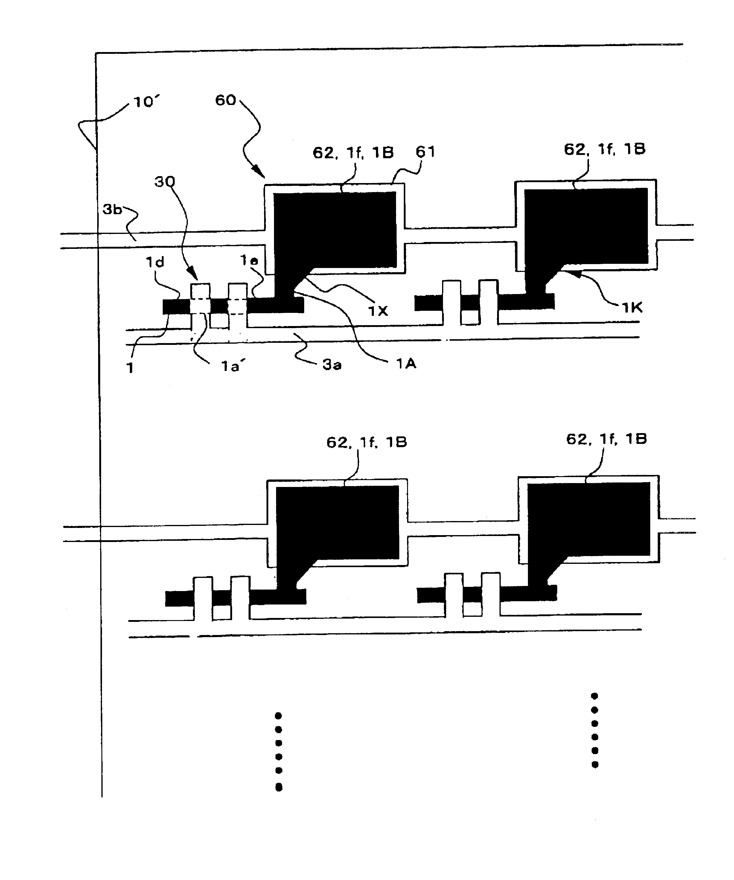
Firstly, for better understanding of the spirit of the present invention, descriptions for a first exemplary embodiment will focus on patterning which is performed in a process in which TFTs and storage capacitors are formed on a glass substrate which will become a TFT array substrate forming an electro-optical device such as a liquid-crystal display device. The electro-optical device, the TFT array substrate and the like serving as components of the device, positions of the TFTs, the storage capacitors, and components forming the TFTs and the storage capacitors in the electro-optical device, etc., are described further below.

TFTs 30 and storage capacitors 60 shown in FIG. 1 are eventually formed on a glass substrate 10′ in the first exemplary embodiment. In FIG. 1, the pluralities of the TFTs 30 and the storage capacitors 60 are formed on the glass substrate 10′ in a matrix array.

Each TFT 30 includes a semiconductor film 1, having a predetermined pattern represented by a black shad...

second exemplary embodiment

Next, in a second exemplary embodiment, a more specific configuration including the TFT 30 and the storage capacitor 60 described in the first exemplary embodiment as components of an electro-optical device is described below. In the following description of this exemplary embodiment, the electro-optical device is applied to a liquid-crystal display device.

(Basic Structure of Electro-optical Device)

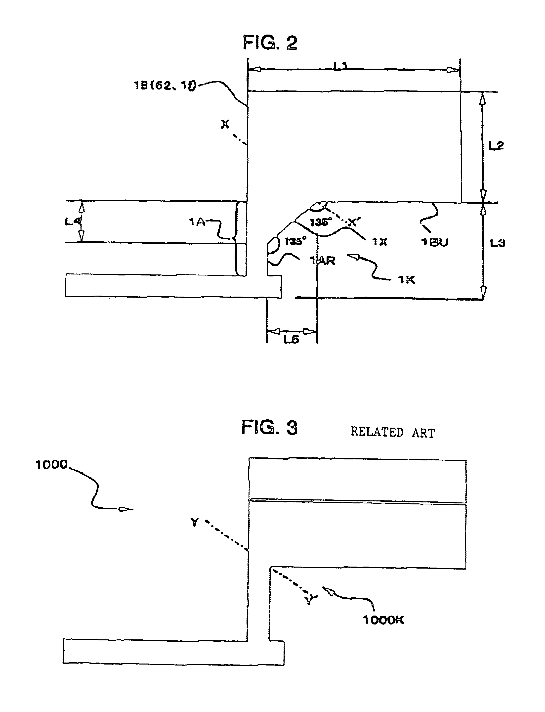
Referring now to FIGS. 12 to 14, the basic structure of the liquid-crystal display device according to the second exemplary embodiment is described below. FIG. 12 is a plan view illustrating a TFT array substrate, together with components formed thereon, viewed from a counter substrate. FIG. 13 is a sectional view taken along plane H-H′ indicated in FIG. 12. Also, FIG. 14 is a schematic circuit diagram of various elements, wiring lines, and so forth disposed in a plurality of pixels, formed in a matrix array, which forms an image display region of the electro-optical device.

In FIGS. 12 an...


PUM

PropertyMeasurementUnit
interior angleaaaaaaaaaa

Abstract

The invention provides a thin-film semiconductor device, which reduces or prevents an undercut from being produced below a thin film when a pattern including an intersection is formed in the thin film. The invention also provides a method of manufacturing the same. A semiconductor film has a pattern including a bent shape or a projected shape. One line segment and another line segment, which define an intersection of the bent shape or the projected shape and which are consecutive, have an additional line segment interposed between ends of the one line segment and the other line segment form a smooth intersection in which each of the angles formed between the additional line segment and the one line segment and between the additional line segment and the other line segment is greater than 90° and less than 180°.

Description

BACKGROUND OF THE INVENTION1. Field of InventionThe present invention relates to thin-film semiconductor devices and methods of manufacturing the same. More specifically, the invention relates to a thin-film semiconductor device, including a thin film which has been formed into a predetermined pattern, and a method of manufacturing the same. Also, the present invention relates to an electro-optical device including such a thin-film semiconductor device, and to a method of manufacturing the same. In addition, the present invention relates to a reticle suitable for use in manufacturing the thin-film semiconductor device and the electro-optical device.2. Description of Related ArtIn the related art, photolithography can be used to form thin-film semiconductor devices. Photolithography is a technique of forming wiring lines, circuit elements, or the like, having a desired pattern, on the surface of a substrate. More particularly, firstly, a thin film composed of, for example, silicon, a...

Claims


Application Information

Patent Timeline
Patent Type & Authority Patents(United States)
IPC IPC(8): G02F1/1362G02F1/13H01L27/12G02F1/1368G02F1/1335G03F1/00G03F1/68G03F7/20H01L21/3205H01L21/336H01L21/768H01L29/786
CPCH01L27/12G02F1/136213H01L21/027
Inventor AMANO, TAKAHIROKITAWADA, KIYOFUMI
Owner BOE TECH GRP CO LTD
Why Eureka
Try Eureka