Organic Light Emitting Display Device and Method for Manufacturing the Same

a technology of light-emitting display and organic materials, which is applied in static indicating devices, instruments, electroluminescent light sources, etc., can solve the problems of serious deformation of reliability of display modules and the inability to evenly plane the cover plate, so as to reduce the step difference and enhance contact reliability and connectivity.

Active Publication Date: 2012-06-07
LG DISPLAY CO LTD
View PDF1 Cites 45 Cited by
  • Summary
  • Abstract
  • Description
  • Claims
  • Application Information

AI Technical Summary

Benefits of technology

[0026]The organic light emitting display device according to some embodiments of the present disclosure is manufactured by forming an organic light emitting diode on a thin organic layer, stacking various films comprising the display module, fixing and connecting the pad and film type printed circuit board with a reinforced adhesive, so that the contact reliability and the connecting reliability are enhanced. Assembling the cover plate using the optical adhesive to reduce the step differences due to the multi stacked structure, the display module panel can be maintained in the evenly plane condition. Furthermore, the present disclosure also provides a display panel module having an organic light emitting diode on a flexible organic substrate and a method for manufacturing the same.

Problems solved by technology

Due to the step differences, the cover plate cannot be assembled in the evenly plane state.
In addition, if, due to the step differences, there are some failures when the COF is attached to the display panel, the reliability of the display module can be seriously degraded.

Method used


Image

  • Organic Light Emitting Display Device and Method for Manufacturing the Same
  • Organic Light Emitting Display Device and Method for Manufacturing the Same
  • Organic Light Emitting Display Device and Method for Manufacturing the Same

Examples


Embodiment Construction

[0031]Reference will be made in detail to the specific embodiments of the present invention, examples of which are illustrated in the accompanying drawings. Wherever possible, the same reference numbers will be used throughout the drawings to refer to the same or like parts. It will be paid attention that detailed description of known arts will be omitted if it is determined that the arts can mislead the present invention.

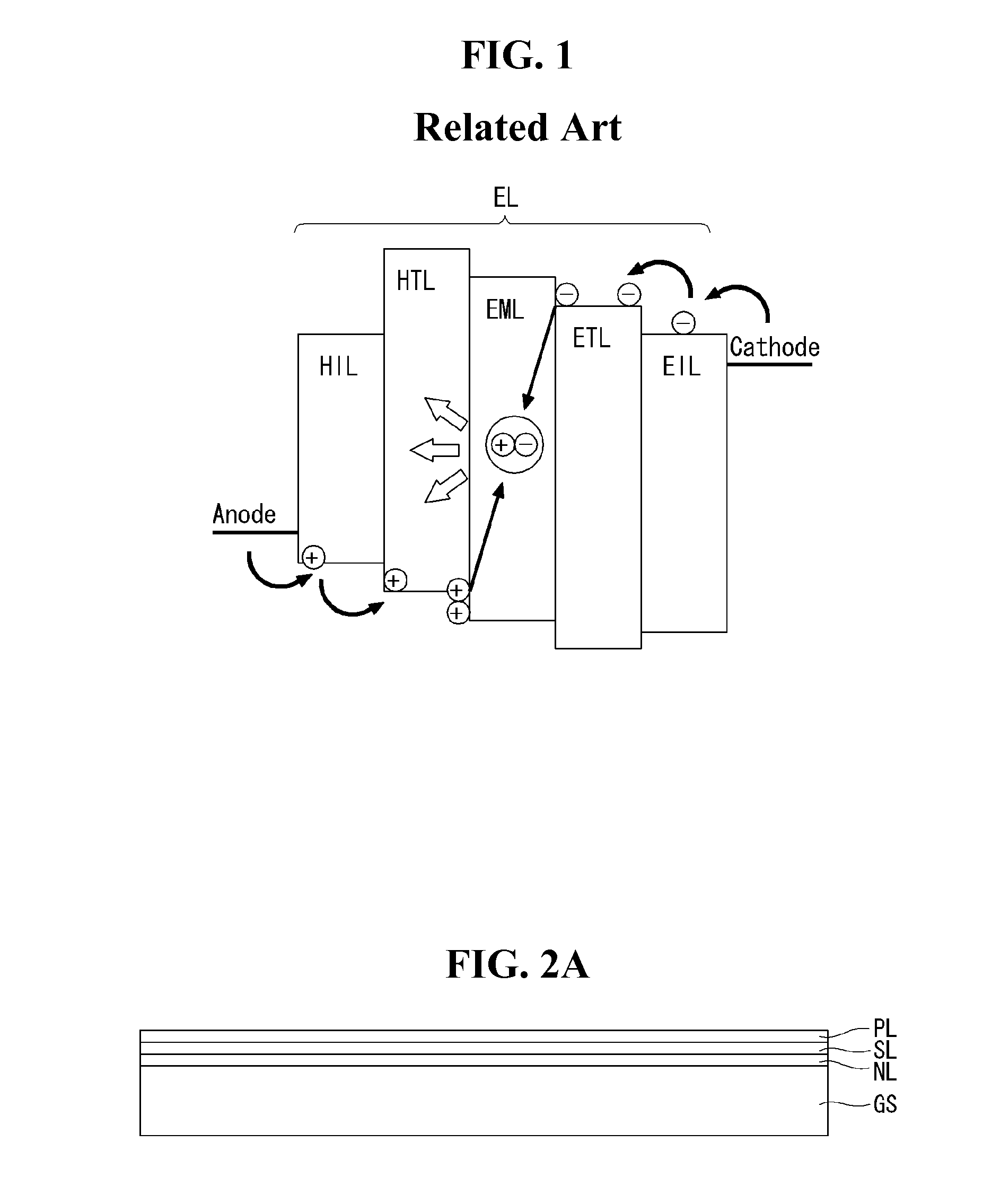
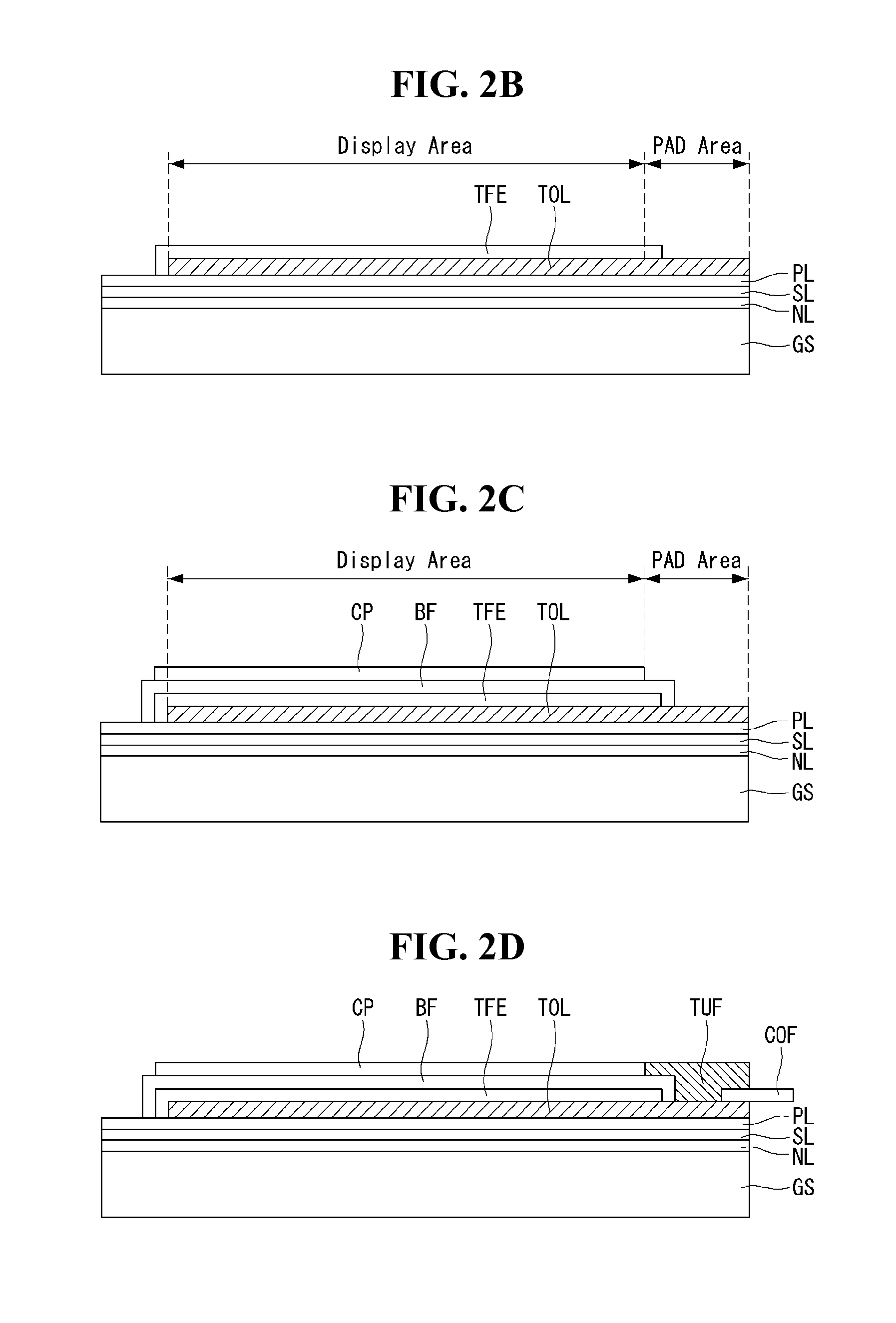
[0032]FIGS. 2A to 3H show some exemplary embodiments of the present disclosure. FIGS. 2A to 2G are cross-sectional views illustrating the exemplary steps of manufacturing a thin active matrix type organic light emitting diode display panel module according to the first embodiment of the present disclosure.

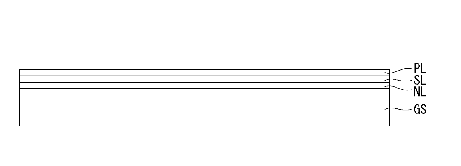
[0033]A base substrate GS having the rigidity enough for forming the display elements having the thin film transistor in stable condition is prepared. Here, the enough rigidity means that the base substrate GS is not bent or deformed so as to make negative effects...


PUM


Abstract

The present disclosure relates to an organic light emitting display device and a method for manufacturing the same. The present disclosure suggests an organic light emitting display device including an organic layer; a display element layer including a display area representing video data and a pad area extended from the display area, on the organic layer; film elements formed on the display element layer; a film type printed circuit board connected to the pad area; and a reinforcing adhesive filling a space between the film type printed circuit board and the film elements

Description

[0001]This application claims the benefit of Korea Patent Application No. 10-2010-0122819 filed on Dec. 3, 2010, which is incorporated herein by reference for all purposes as if fully set forth herein.BACKGROUND OF THE INVENTION[0002]1. Field of the Invention[0003]The present disclosure relates to an organic light emitting display device (or, OLED) and a method for manufacturing the same. Especially, the present disclosure relates to an organic light emitting display device including active organic light emitting diodes on a flexible substrate and a method for manufacturing the same.[0004]2. Discussion of the Related Art[0005]Nowadays, various flat panel display devices are developed for overcoming many drawbacks of the cathode ray tube, such as heavy weight and bulk volume. The flat panel display devices include the liquid crystal display device (or LCD), the field emission display (or FED), the plasma display panel (or PDP) and the electroluminescence display device (or ED).[0006]...

Claims


Application Information

Patent Timeline
Patent Type & Authority Applications(United States)
IPC IPC(8): G09G3/30H01L33/52
CPCH01L51/5253H05B33/00H10K50/844H10K50/80H10K71/00H10K50/841H10K50/868H10K71/80H10K2102/00H10K2102/311
Inventor KIM, JONGMOOYOO, JUHNSUK
Owner LG DISPLAY CO LTD
Why Eureka
Try Eureka