Reduced circuit trace roughness for improved signal performance

a circuit trace and roughness technology, applied in the field of signal transmission, can solve the problems of reducing signal reach and performance, conductive circuit traces often exhibit surface roughness, etc., and achieve the effect of improving signal performance, reducing both lateral and transverse fabrication roughness, and improving high-speed signal propagation

Inactive Publication Date: 2012-06-21
RPX CLEARINGHOUSE
View PDF6 Cites 3 Cited by
  • Summary
  • Abstract
  • Description
  • Claims
  • Application Information

AI Technical Summary

Benefits of technology

[0006]According to the present invention, a technique for improving signal performance in conductive circuit traces is provided. The technique may be realized by the use of chemical polishing, electropolishing, or other polishing technique to achieve a polished finish by reducing both lateral and transverse fabrication roughness. Surface polishing, along with the use of low profile adhesion promoters substantially improves high speed signal propagation for metal on dielectric circuit boards.
[0007]In one embodiment, the technique may be realized as a method for improving performance of a signal transmitted via a conductive circuit trace of a circuit board. The method comprises the step of reducing a surface roughness of at least one surface of the conductive circuit trace.

Problems solved by technology

Conductors, however, frequently exhibit a surface roughness that may extend into the skin depth of the conductors.
This increase in the effective signal path results in a corresponding increase in the resistance to the flow of the current and transmission time and, consequently, a decrease in the signal reach and performance.

Method used


Image

  • Reduced circuit trace roughness for improved signal performance
  • Reduced circuit trace roughness for improved signal performance
  • Reduced circuit trace roughness for improved signal performance

Examples


Embodiment Construction

)

[0017]The following description is intended to convey a thorough understanding of the present invention by providing a number of specific embodiments and details involving polishing conductive circuit traces in circuit boards and other circuit devices. It is understood, however, that the present invention is not limited to these specific embodiments and details, which are exemplary only. It is further understood that one possessing ordinary skill in the art, in light of known systems and methods, would appreciate the use of the invention for its intended purposes and benefits in any number of alternative embodiments, depending upon specific design and other needs.

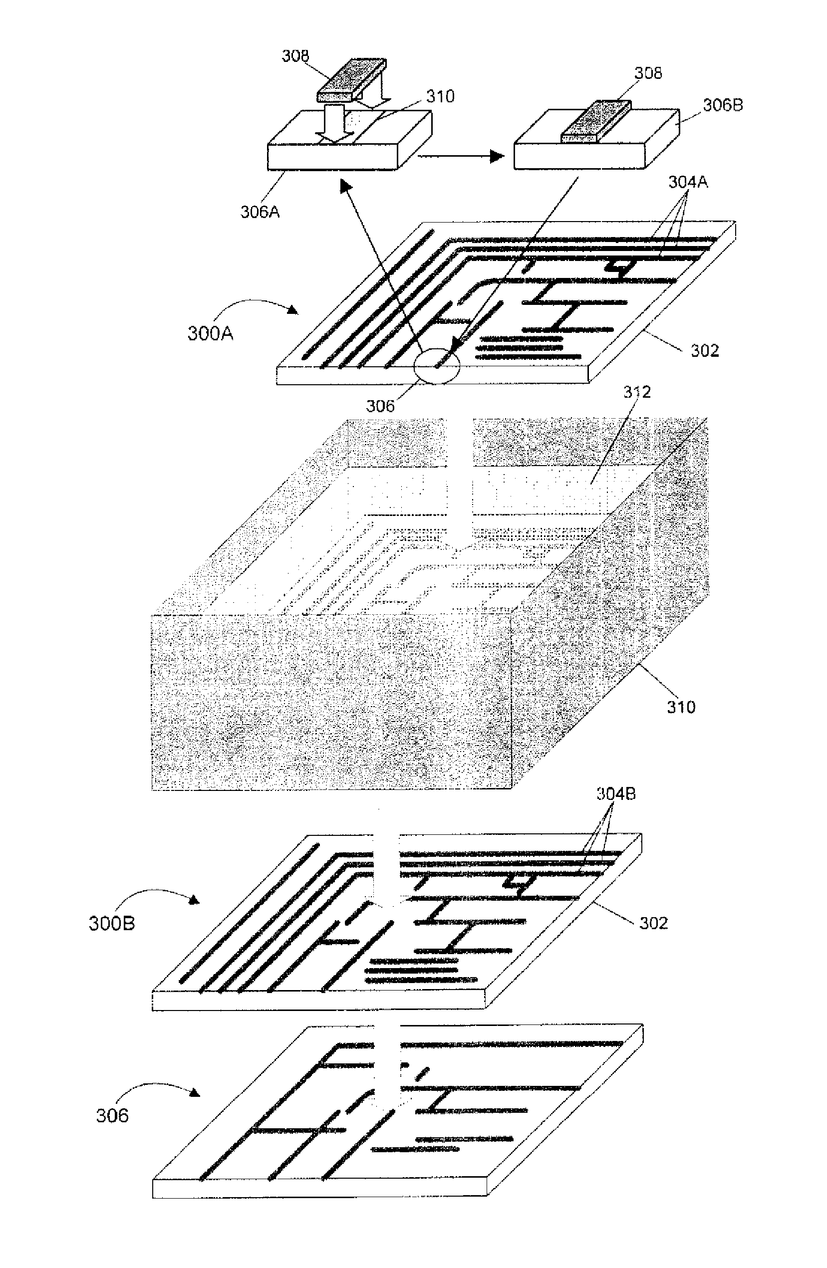
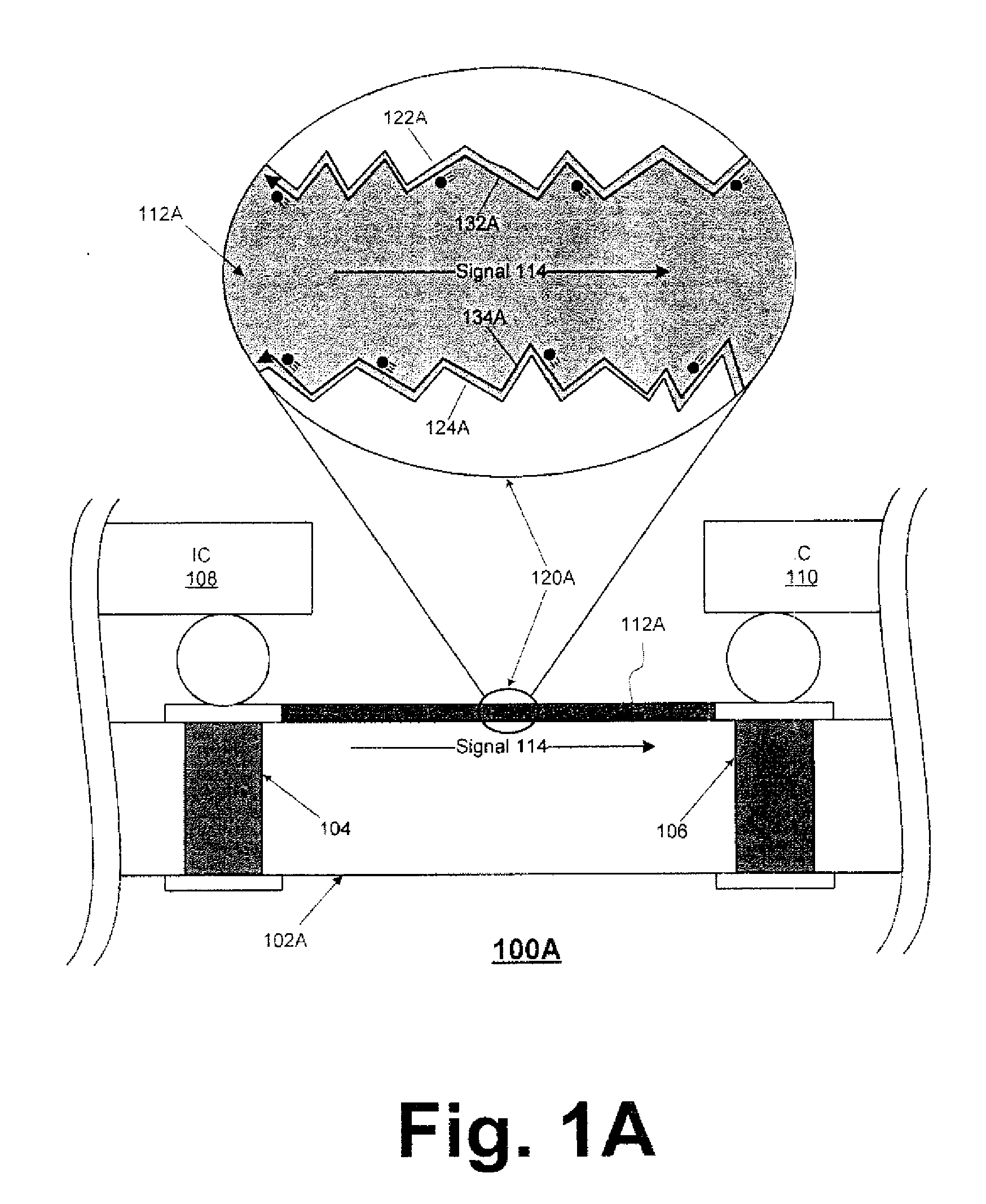
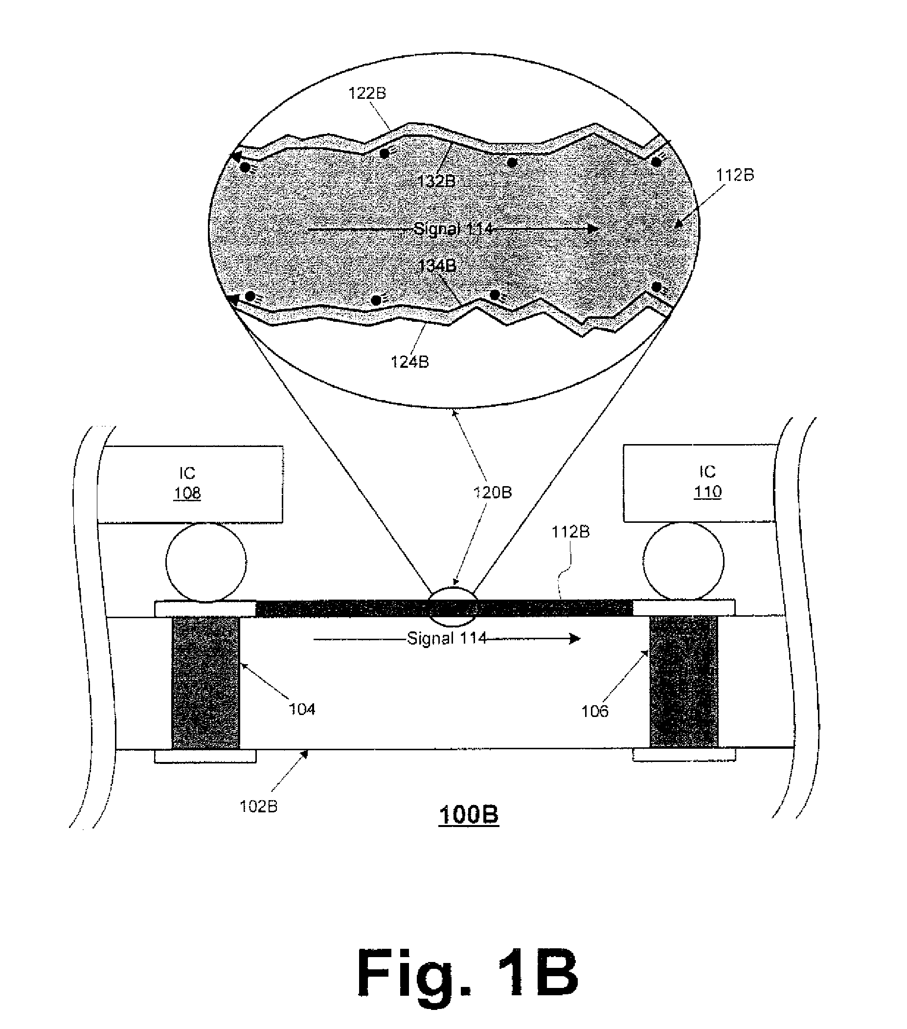
[0018]FIGS. 1A-3 illustrate various exemplary techniques for polishing circuit traces of a printed circuit board (PCB) to improve the performance of signals transmitted therein. In at least one embodiment, one or more surfaces of one or more conductive circuit traces of a PCB may be polished to reduce their surface roughne...


PUM

PropertyMeasurementUnit
skin depthaaaaaaaaaa

Abstract

Exemplary techniques for improving the performance of signals transmitted by conductive circuit traces are disclosed. The techniques may be realized as a method comprising the step of reducing a surface roughness of at least one surface of a conductive circuit trace. Alternatively, the techniques may be realized as a circuit board for transmitting at least one signal, the circuit board comprising at least one conductive circuit trace for carrying at least one signal, the at least one conductive circuit trace having at least one polished surface. Further, the technique may be realized as a conductive circuit trace for carrying a signal, the conductive circuit trace comprising conductive material having a plurality of surfaces substantially parallel with a direction of propagation of the signal, wherein the plurality of surfaces includes at least one polished surface having a reduced surface roughness.

Description

CROSS-REFERENCE TO RELATED APPLICATIONS[0001]This patent application is a continuation of U.S. patent application Ser. No. 10 / 667,491 filed Sep. 23, 2003, now U.S. Pat. No. 8,123,927, issued Feb. 28, 2012 which is hereby incorporated by reference herein in its entirety.FIELD OF THE INVENTION[0002]The present invention relates generally to signal transmission via circuit traces in single-layer or multilayer circuit boards and, more particularly, to a technique for reducing the surface roughness of a circuit trace to improve the performance of a signal transmitted therein.BACKGROUND OF THE INVENTION[0003]Conductors transmitting signals often exhibit a phenomenon known as “skin effect” whereby the self-inductance of the conductors forces electrons toward the surface of the conductors. Skin effect is particularly prevalent in conductors transmitting high-frequency signals. For example, it has been found that for a copper conductor, the depth from the surface at which the majority of the...

Claims


Application Information

Patent Timeline
Patent Type & Authority Applications(United States)
IPC IPC(8): H05K1/00B32B38/10B32B38/00
CPCH05K1/0242H01L2224/16227H01L2924/15192H01L2924/15313
Inventor SHEFFIELD, ROBERTGOULET, EILEEN
Owner RPX CLEARINGHOUSE
Why Eureka
Try Eureka