Touch panel touching sensing integration structure

A touch panel and touch sensing technology, applied in the input/output process of data processing, instruments, electrical and digital data processing, etc. The effect of conductivity, increasing signal transmission capacity, and increasing market competitiveness

Active Publication Date: 2015-01-14
INTERFACE OPTOELECTRONICS SHENZHEN +1
View PDF3 Cites 3 Cited by
  • Summary
  • Abstract
  • Description
  • Claims
  • Application Information

AI Technical Summary

Problems solved by technology

[0003] However, the single-piece glass touch panel is mostly made of a black frame photoresist material or black matrix material (Black Matrix; BM), or is made of a colored layer, such as figure 1 As shown, it is a schematic diagram of the integrated structure of the touch panel in the prior art. Most of them use multi-layer ink (Ink) material and screen printing process to make the black matrix material, but the indium tin oxide wire 14 must be formed from the structure of the touch panel 10. The bottom forms a ramp through the multi-layer ink layer 12 and climbs to the uppermost ink layer. During the climbing process of the indium tin oxide wire, it is easy to reach point A at the junction of the ink layer 12 and the ink layer 12 due to landform problems and material factors. And cracks occur, which in turn leads to the problem of circuit breakage, which makes the circuit short circuit, the touch function fails, and the number of spot tests decreases, so it cannot be integrated into the touch panel and other technical bottlenecks.

Method used


Image

  • Touch panel touching sensing integration structure
  • Touch panel touching sensing integration structure
  • Touch panel touching sensing integration structure

Examples


Embodiment Construction

[0026] It should be understood that the specific embodiments described here are only used to explain the present invention, not to limit the present invention.

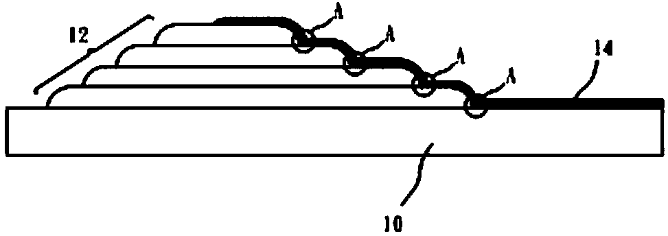
[0027] With the vigorous development of the touch panel industry in recent years, in order to make the touch panel more humanized and convenient, it has gradually entered the small, compact, light and thin generation. Therefore, in order to meet the design requirements of lightness and low price, and greatly Simplify the structure of the touch sensing layer and lower the production cost. The touch sensing integrated structure of the touch panel designed in the present invention is a monolithic glass touch panel, and a piece of glass is used as the surface cover glass and the touch panel. The substrate of the control sensor, and through the design ingenuity that does not affect the visibility of the panel, the product is more reliable, in order to increase the market competitiveness.

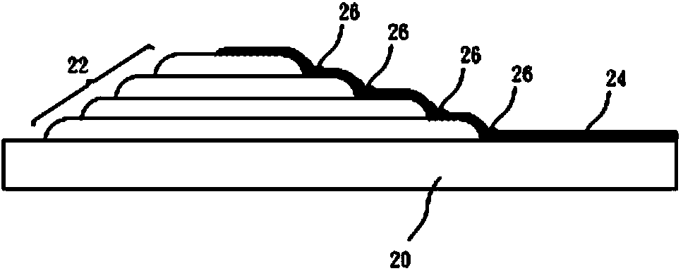
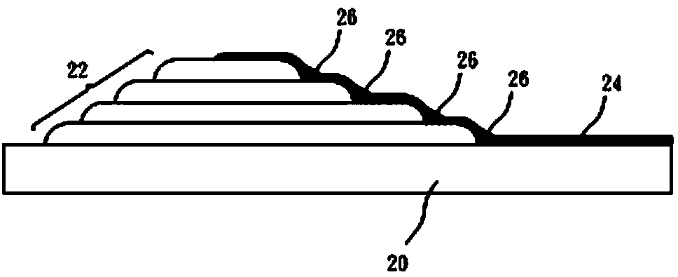
[0028] Such as figure 2 As show...


PUM


Abstract

The invention discloses a touch panel touching sensing integration structure. A plurality of ink layers are stacked on a transparent substrate in a screen printing manner, at least one guide wire is arranged on the transparent substrate and extends to the surface of the ink layer of the top along each ink layer, and a conductive stacking layer is arranged at the connection of each of two adjacent ink layers and is located on the guide wire. Thus, fine metal ductility and conductivity can be achieved through small conductive stacking layers without affecting the visibility, and the signal transduction capacity of the guide wires is improved.

Description

technical field [0001] The invention relates to the technical field of touch sensing, in particular to a touch sensing integration structure of a touch panel. Background technique [0002] At present, in order to meet the needs of consumers for thinner and lighter touch panels, the current projected capacitive touch panel thinning solution is directed towards the development of integrated sensor patterns to reduce the amount of ITO glass and ITO thin film. In terms of the One Glass Solution (OGS) technology, the indium tin oxide glass and the protective cover glass are integrated into one piece of glass, that is, the sensor pattern is directly made on the protective cover glass, so It can reduce one piece of glass and save one bonding process. [0003] However, the single-piece glass touch panel is mostly made of a black frame photoresist material or black matrix material (Black Matrix; BM), or is made of a colored layer, such as figure 1 As shown, it is a schematic diagra...

Claims


Application Information

Patent Timeline
Patent Type & Authority Applications(China)
IPC IPC(8): G06F3/041G06F3/044
CPCG06F3/041G06F3/044G06F2203/04103
Inventor 辛坤莹陈宗凯黄彦衡
Owner INTERFACE OPTOELECTRONICS SHENZHEN
Why Eureka
Try Eureka