Space transformer and manufacturing method thereof

a technology of space transformer and manufacturing method, which is applied in the field of space transformer, can solve the problem of the fine pitch of the device for probing or testing such highly integrated semiconductor dies, and achieve the effect of increasing the manufacturing efficiency of space transformer and simplifying the structure of the test probe apparatus

Active Publication Date: 2020-01-30
HU DYI CHUNG
View PDF0 Cites 3 Cited by
  • Summary
  • Abstract
  • Description
  • Claims
  • Application Information

AI Technical Summary

Benefits of technology

[0004]The invention provides a space transformer and a manufacturing method thereof. The space transformer configured to connect a signal source and probe a semiconductor wafer provides a fine circuitry side for mating with the probe pins and a coarse circuitry side for mating with the signal source, thereby simplifying of a structure of test probe apparatus and increasing manufacturing efficiency of a space transformer.
[0009]Based on the above, the space transformer includes the fine contact pads of the redistribution structure formed according to the IC design rules such that the probe side of the space transformer can meet the requirements of fine-pitch spacing of the testing probes which are used to probe or test the semiconductor wafer. The space transformer further includes the coarse contact pads of the circuit board formed according to the PCB design rules such that the signal source side of the space transformer can mate with the testing PCB for transmitting the signal to the probe side. In addition, the conductive through vias provide vertical conductive paths in the space transformer, thereby shortening signal length and minimizing a noise between operations so as to improve a signal performance of the testing apparatus.

Problems solved by technology

The testing pad pitches of highly integrated semiconductor die has become narrower, whereas the degree to which a device for probing or testing such highly integrated semiconductor dies can have a fine pitch is limited.

Method used


Image

  • Space transformer and manufacturing method thereof
  • Space transformer and manufacturing method thereof
  • Space transformer and manufacturing method thereof

Examples


Embodiment Construction

[0016]Reference will now be made in detail to the present preferred embodiments of the invention, examples of which are illustrated in the accompanying drawings. Wherever possible, the same reference numbers are used in the drawings and the description to refer to the same or like parts.

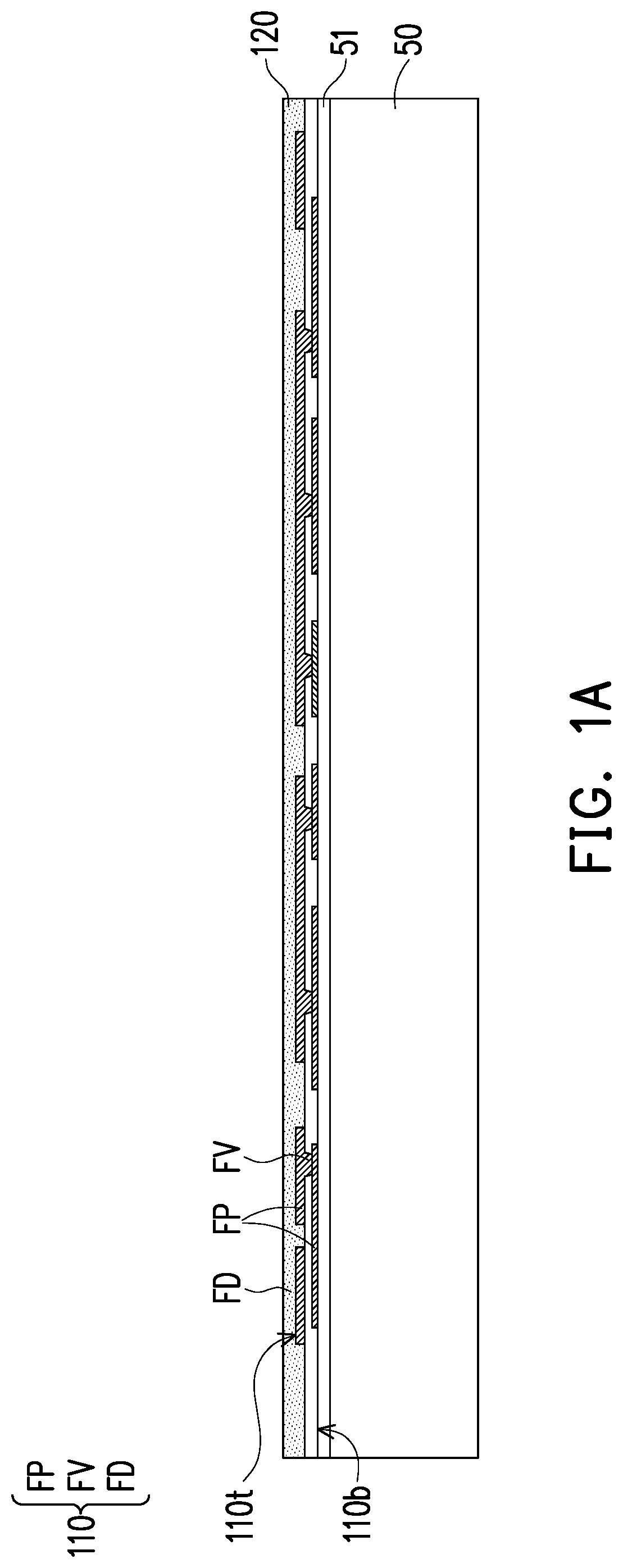
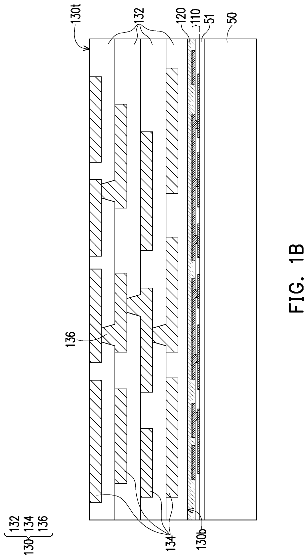
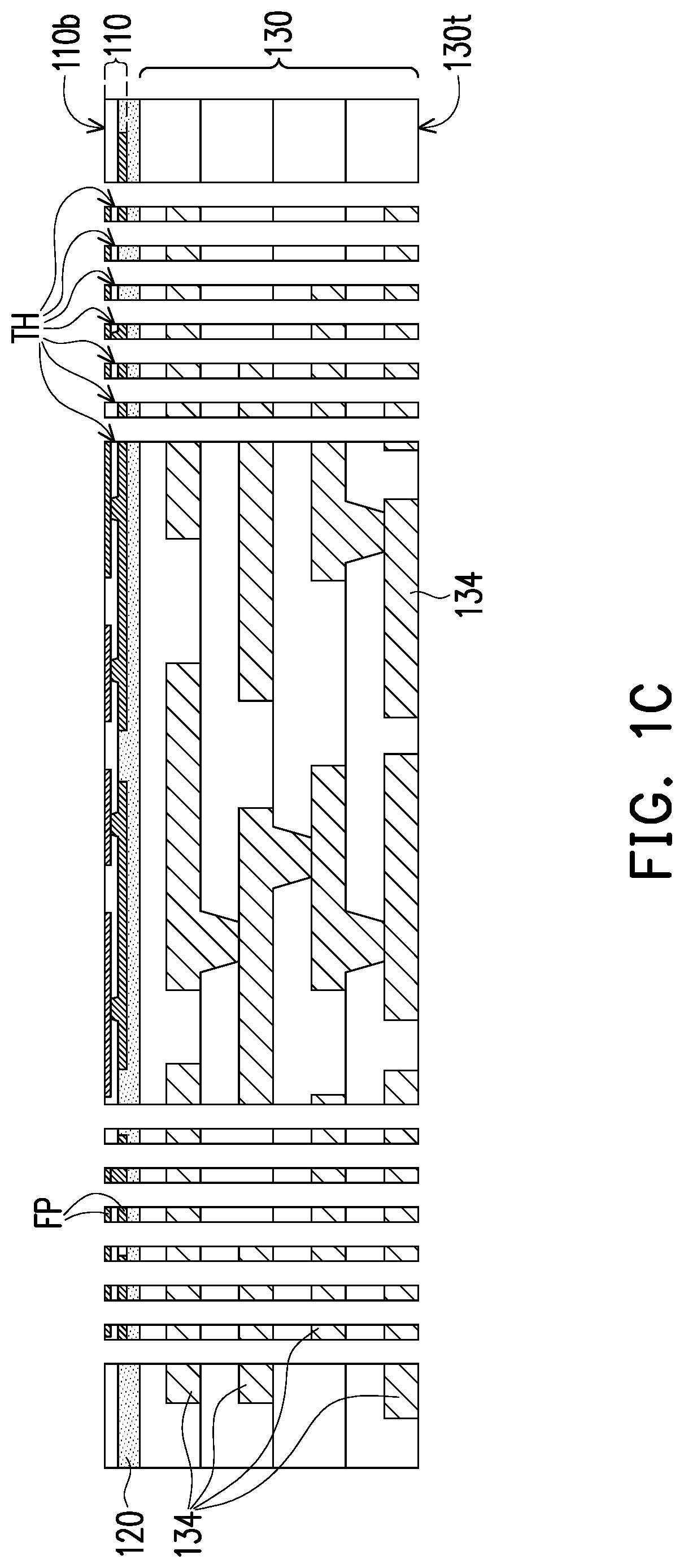
[0017]FIG. 1A to FIG. 1D are schematic cross-sectional views illustrating a manufacturing method of a space transformer according to some embodiments of the invention. Referring to FIG. 1A, a redistribution structure 110 is formed over a temporary carrier 50 and a bonding layer 120 is formed over the redistribution structure 110. The temporary carrier 50 may be made of glass, plastic, silicon, metal, or other suitable materials as long as the material is able to withstand the subsequent processes while carrying a structure formed thereon. In some embodiments, a release layer 51 (e.g., a light to heat conversion film, or other suitable de-bonding layer) may be applied on a top surface of the temporary...


PUM


Abstract

A space transformer for connecting a signal source and probing a semiconductor wafer and a manufacturing method thereof are provided. The space transformer includes a circuit board including a wiring structure, a redistribution structure bonded to the circuit board and including second contact pads configured to probe the semiconductor wafer, a conductive through via penetrating through the circuit board and providing a vertical conductive path between the circuit board and redistribution structure. A plurality of first contact pads of the wiring structure is configured to connect the signal source. The redistribution structure is thinner than the circuit board, wherein a pitch of the adjacent second contact pads is finer than that of the adjacent first contact pads.

Description

CROSS REFERENCE TO RELATED APPLICATION[0001]This application claims the priority benefit of U.S. provisional application Ser. No. 62 / 711,628, filed on Jul. 30, 2018. The entirety of the above-mentioned patent application is hereby incorporated by reference herein and made a part of specification.BACKGROUND OF THE INVENTION1. Field of the Invention[0002]The present invention relates to a space transformer, and more specifically relates to a space transformer for connecting a signal source and probing a semiconductor wafer.2. Description of Related Art[0003]As the electronic industry has rapidly developed, the trend in semiconductor dies has been to gradually move toward miniaturization and integration. The testing pad pitches of highly integrated semiconductor die has become narrower, whereas the degree to which a device for probing or testing such highly integrated semiconductor dies can have a fine pitch is limited. In this respect, a space transformer to support fine testing pad p...

Claims


Application Information

Patent Timeline
Patent Type & Authority Applications(United States)
IPC IPC(8): G01R1/073G01R31/26H05K3/40H05K3/42H05K1/11
CPCH05K1/114H05K3/429G01R1/07378H05K3/4007G01R31/2601H01L23/5389H01L23/49816H01L23/5383H01L23/5384G01R31/2889G01R3/00H05K3/3436H05K2201/10378H01L2224/2518H01L2224/81005H01L2924/181H01L2924/15311H01L2224/73204H01L2224/32225H01L2224/13025H01L2224/92225H01L2224/73259H01L2224/16225H01L24/19H01L2924/00014H01L24/20H01L24/81H01L24/83H01L24/92H01L24/73H01L2224/92125H01L24/24H01L24/82H01L24/16H01L24/32H01L2224/17106H01L24/17H01L24/25H01L25/50H01L25/105H01L25/0655H01L2924/00012H01L2224/13099H01L2224/29099H01L23/49827H01L21/4853H01L21/486H01L24/08H01L2224/02373H01L23/481H01L2224/02372H01L23/49838
Inventor HU, DYI-CHUNG
Owner HU DYI CHUNG
Why Eureka
Try Eureka