
Semiconductor device and method for forming the same

a semiconductor memory and semiconductor technology, applied in the field of semiconductor memory devices, can solve the problems of reducing the overall area of a complicated semiconductor memory apparatus, and achieve the effects of preventing a floating body effect, preventing isolation, and sufficient-sized overlap regions

Inactive Publication Date: 2012-06-21
SK HYNIX INC
View PDF1 Cites 0 Cited by
  • Summary
  • Abstract
  • Description
  • Claims
  • Application Information

AI Technical Summary

Benefits of technology

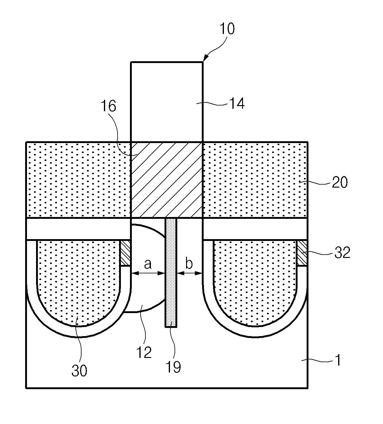
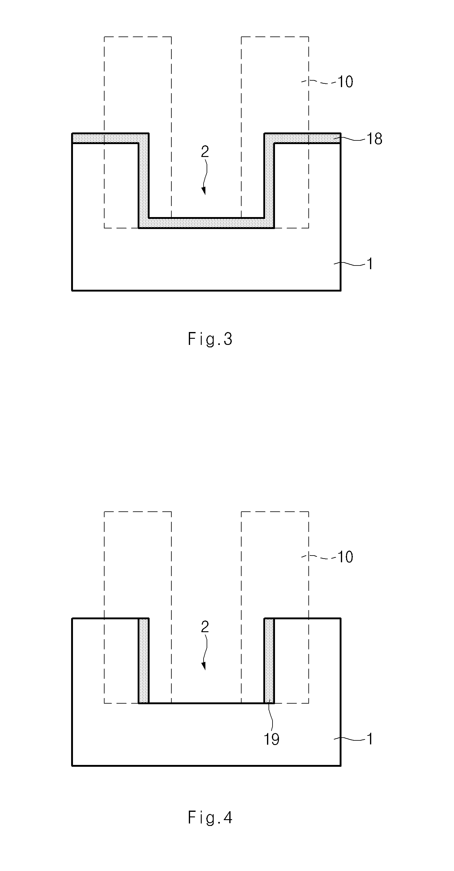
The present invention provides a semiconductor device and method for forming the same that overcome limitations and disadvantages of conventional art. Specifically, the invention includes a diffusion control layer formed at the center of a vertical pillar to prevent isolation between a channel region and a semiconductor substrate and to prevent the floating body effect. The invention also guarantees a sufficient-sized overlapping region between a gate and a junction region. The diffusion control layer may include an oxide film or a nitride film and can be formed by etching a semiconductor substrate and burying an insulation film. The invention further includes a bit line and a word line formed at a lateral surface of the vertical pillar. These technical effects improve the performance and reliability of semiconductor devices.

Problems solved by technology

Reducing the overall area of a complicated semiconductor memory apparatus is difficult due to the plurality of transistors contained in the semiconductor device.

Method used


Image

  • Semiconductor device and method for forming the same
  • Semiconductor device and method for forming the same
  • Semiconductor device and method for forming the same

Examples


Embodiment Construction

[0027]Reference will now be made in detail to an embodiment of the present invention, examples of which are illustrated in the accompanying drawings. Wherever possible, the same reference numerals will be used throughout the drawings to refer to the same or like parts. A semiconductor device and a method for forming the same according to an embodiment of the present invention will hereinafter be described with reference to the appended drawings.

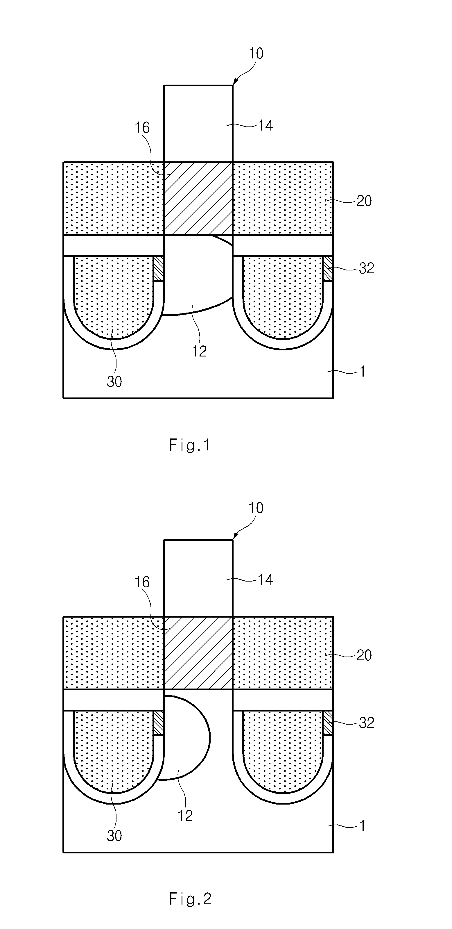
[0028]FIGS. 1 and 2 show problems encountered in a conventional vertical pillar structure. Referring to FIGS. 1 and 2, the semiconductor device includes a vertical pillar 10 vertically extending from a semiconductor substrate 1. Sequentially, from the bottom of the vertical pillar, the semiconductor device includes a first junction region 12, a channel region 16, and a second junction region 14. The first junction region 12 and the second junction region 14 operate as a source and a drain of the transistor, respectively. In the above-mentione...


PUM


Abstract

A semiconductor device and a method for forming the same are disclosed. The semiconductor device prevents separation between the channel region and the semiconductor substrate to prevent the floating body effect and to guarantee a sufficient overlap between a gate and a junction region. The semiconductor device includes a vertical pillar including a vertical channel, a diffusion control layer contained in the vertical pillar, and a junction region formed close to the diffusion control layer in the vertical pillar.

Description

CROSS-REFERENCE TO RELATED APPLICATION[0001]The priority of Korean patent application No. 10-2010-0128576 filed on 15 Dec. 2010, the disclosure of which is hereby incorporated in its entirety by reference, is claimed.BACKGROUND OF THE INVENTION[0002]Embodiments of the present invention relate to a semiconductor device and a method for forming the same, and more particularly, to a semiconductor device that has a vertical channel and a method for forming the same.[0003]Generally, a semiconductor is a material that could be made conductive by providing dopants into the material. Although a semiconductor is similar to a nonconductor in a pure state, the electric conductivity of a semiconductor device is increased by impurity implantation or other manipulation. The semiconductor is used to form a semiconductor device, such as a transistor, through impurity implantation and a wire interconnection. A device that has various functions simultaneously while being formed of a semiconductor ele...

Claims


Application Information

Patent Timeline
Patent Type & Authority Applications(United States)
IPC IPC(8): H01L29/78H01L21/336
CPCH01L27/10876H01L27/10885H01L29/7827H01L29/66666H01L29/0653H10B12/053H10B12/482H10B12/395
Inventor KIM, JUNG NAM
Owner SK HYNIX INC
Learn More