
Method for manufacturing silicon-on-insulator (SOI) complementary metal oxide semiconductor (CMOS) device with vertical gate structure

A fabrication method, vertical gate technology, applied in semiconductor/solid-state device manufacturing, semiconductor devices, electrical components, etc.

Inactive Publication Date: 2012-07-11
SHANGHAI INST OF MICROSYSTEM & INFORMATION TECH CHINESE ACAD OF SCI +1
View PDF2 Cites 0 Cited by
  • Summary
  • Abstract
  • Description
  • Claims
  • Application Information

AI Technical Summary

Problems solved by technology

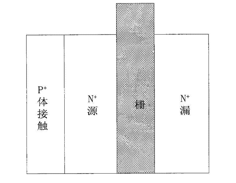
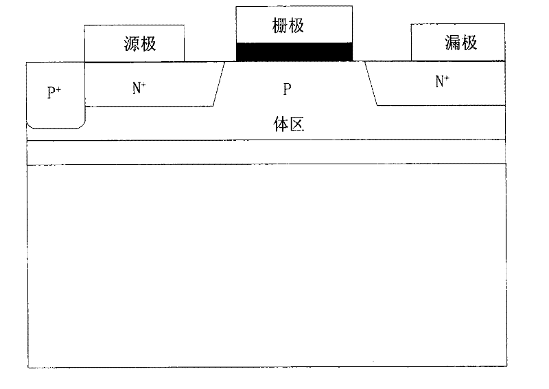
The traditional volume lead structure such as Figure 1, 2, the P formed on the left side of the source area The + injection region is connected to the P-type body region below the source region. When the MOS device is working, the carriers accumulated in the body region are released through the P+ channel to reduce the potential of the body region. Purpose; but this method complicates the process flow and increases parasitic effects, which not only reduces some electrical properties but also increases the device area

Method used


Image

  • Method for manufacturing silicon-on-insulator (SOI) complementary metal oxide semiconductor (CMOS) device with vertical gate structure
  • Method for manufacturing silicon-on-insulator (SOI) complementary metal oxide semiconductor (CMOS) device with vertical gate structure
  • Method for manufacturing silicon-on-insulator (SOI) complementary metal oxide semiconductor (CMOS) device with vertical gate structure

Examples


Embodiment 1

[0042] 1. Use STI technology to perform oxide isolation on the PMOS region and the NMOS region.

[0043] 2. A window is etched between the PMOS area and the NMOS area, and other parts are protected with photoresist, and the sidewall is oxidized by thermal oxidation to form the gate oxide layer of PMOS and NMOS, and then polysilicon is deposited at the window, Fill, dope, chemical mechanical polish CMP.

[0044] 3. The channels of NMOS and PMOS are doped by multiple ion implantation. After doping, rapid annealing is performed. The vertical depth can be adjusted by adjusting the implantation energy and dose. After the doping is completed, the profile impurities should be evenly distributed, and the impurity distribution at the edge is clear and steep.

[0045] 4. The source region and the drain region of NMOS and PMOS are heavily doped by ion implantation, and rapid annealing is performed after doping.

[0046] 5. After etching windows for the channel, source region, drain reg...

Embodiment 2

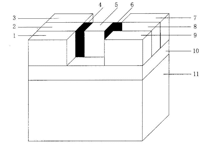
[0058] The SOI substrate includes a silicon substrate layer 11 grown from bottom to top, a buried oxide layer 10, and a single crystal silicon top layer. Both the NMOS gate oxide layer 4 and the PMOS gate oxide layer 6 extend down to the buried oxide layer 10; the vertical gate region 5, the NMOS region, the PMOS region and the silicon substrate layer 11 are separated by the buried oxide layer 10 . The NMOS region includes an NMOS source region 1, an NMOS drain region 3, and an NMOS channel 2. The NMOS source region 1 leads to an NMOS source 16, the NMOS drain region 3 leads to an NMOS drain 14, and the NMOS channel 2 leads to an NMOS body electrode 12. The PMOS region includes a PMOS source region 9, a PMOS drain region 7, and a PMOS channel 8. The PMOS source region 9 leads to a PMOS source 17, the PMOS drain region 7 leads to a PMOS drain 15, and the PMOS channel 8 leads to a PMOS body. electrode 13. A gate 18 leads out from the vertical gate region 5 . The vertical gat...


PUM


Abstract

The invention discloses a method for a silicon-on-insulator (SOI) complementary metal oxide semiconductor (CMOS) device with a vertical gate structure. The method comprises the following steps of: growing a silicon substrate layer, a buried oxide layer, and a monocrystalline silicon top layer in turn from bottom to top; performing oxide isolation in an active area formed on the monocrystalline silicon top layer by using an STI process, wherein the active area comprises an NMOS area and a PMOS area; etching a window between the NMOS area and the PMOS area, and forming an NMOS gate oxide layer and a PMOS gate oxide layer on an inside wall of the window by using a thermal oxidation process; depositing, filling and doping polysilicon at the window, and forming a vertical gate area through chemical-mechanical polishing; and doping and rapidly annealing at an NMOS channel and a PMOS channel through repeated ion implantation, and heavily doping in a source-drain area through ion implantation. The method has the advantages of simple process, capability of manufacturing a device with small occupied area and few pattern layers, no floating-body effect, and convenient test for parasitic resisters and capacitors.

Description

technical field [0001] The invention belongs to the technical field of microelectronics and solid electronics, and relates to a method for manufacturing an SOICMOS device with a vertical gate structure. Background technique [0002] A complementary metal oxide semiconductor (Complementary Metal Oxide Semiconductor, CMOS) device is a semiconductor device that integrates an N-type metal oxide semiconductor transistor (NMOS) and a P-type metal oxide semiconductor transistor (PMOS) on the same silicon chip. With the continuous shrinking of device size, the short channel effect (SCE) has become an insurmountable obstacle for further scaling down of all conventional planar CMOS devices. It leads to the degradation of device characteristics and the increase of parasitic effects, which limits the further development of conventional planar CMOS devices. zoom out. [0003] Silicon On Insulator (Silicon On Insulator, SOI) refers to the substrate technology that replaces the traditiona...

Claims


Application Information

Patent Timeline
Patent Type & Authority Patents(China)
IPC IPC(8): H01L21/84H01L21/768H01L21/28
Inventor 程新红何大伟俞跃辉肖德元王中健徐大朋
Owner SHANGHAI INST OF MICROSYSTEM & INFORMATION TECH CHINESE ACAD OF SCI
Learn More