
Silicon device on insulator and preparation method thereof

A technology of silicon-on-insulator and devices, applied in the field of silicon-on-insulator devices and their preparation, can solve the problems of inability to effectively suppress the floating body effect, deterioration of device performance, reduction of channel width, etc., and to improve the resistance to single particle and transient The ability to irradiate, the effect of reducing power consumption, increasing speed

Active Publication Date: 2011-04-06
INST OF MICROELECTRONICS CHINESE ACAD OF SCI
View PDF0 Cites 0 Cited by
  • Summary
  • Abstract
  • Description
  • Claims
  • Application Information

AI Technical Summary

Problems solved by technology

[0006] The present invention aims at the fact that the T-type gate and H-type gate technologies in the prior art cannot effectively suppress the floating body effect, and the wider the channel, the greater the body resistance, the more significant the floating body effect, and the source-drain asymmetry of the BTS structure, so that the source-drain cannot be interchanged , the effective channel width is reduced, and the contact of the source end introduces a large parasitic capacitance, which makes the performance of the device worse. A silicon-on-insulator device and its preparation method are provided.

Method used


Image

  • Silicon device on insulator and preparation method thereof
  • Silicon device on insulator and preparation method thereof
  • Silicon device on insulator and preparation method thereof

Examples


Embodiment 1

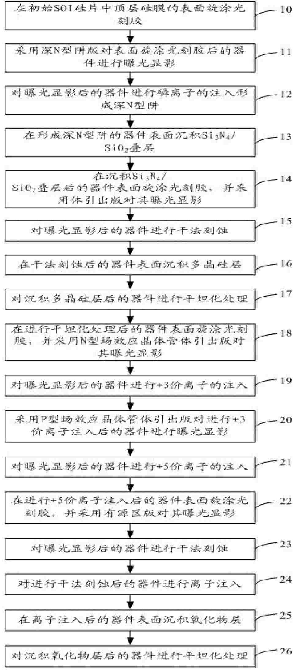
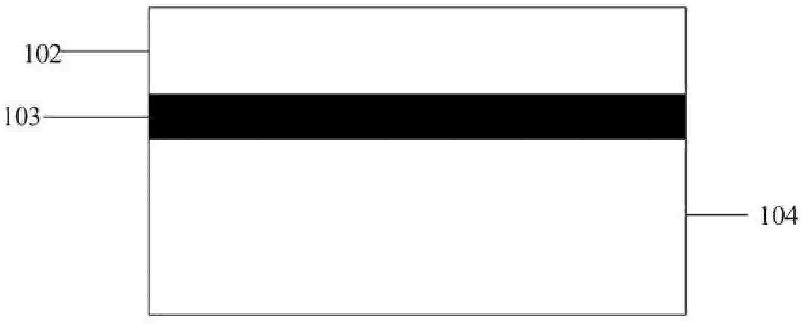
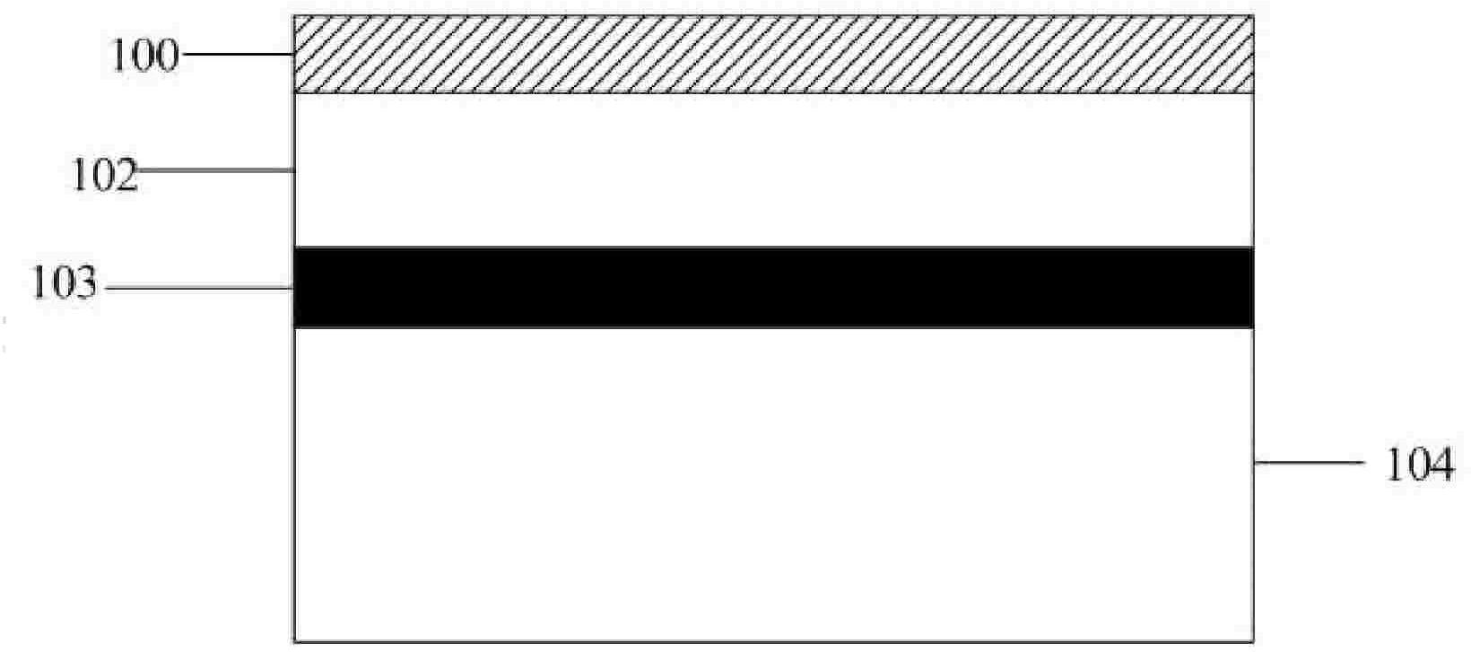
[0052] figure 1 It is a flow chart of a method for preparing a silicon-on-insulator device using shallow trench isolation technology in Embodiment 1 of the present invention. like figure 1 As shown, the silicon-on-insulator device is fabricated by shallow trench isolation (STI isolation technology). The STI isolation technology can provide electrical isolation for different CMOS devices. Although this embodiment adopts the STI isolation technology to form the silicon-on-insulator device, the formation of the silicon-on-insulator device does not depend on the STI isolation technology. According to this embodiment, local silicon oxidation isolation (LOCOS isolation) can also be used. The silicon-on-insulator device is prepared using the MESA isolation technology or mesa isolation technology. The method for preparing the silicon-on-insulator device by adopting shallow trench isolation technology includes the following steps:

[0053] Step 10: Spin-coat photoresist 100 on the ...

Embodiment 2

[0089] Figure 24 It is a schematic diagram of the basic structure of a silicon-on-insulator device fabricated by shallow trench isolation technology in Example 2 of the present invention. like Figure 24 As shown, the figure is also Figure 20 Schematic diagram of the structure along the X-X' direction. The SOI device includes a bottom silicon substrate 104 , a buried oxide layer 103 , and an N-type field effect transistor 66 and a P-type field effect transistor 68 formed in the top layer silicon film 102 . The N-type field effect transistor 66 is located in the body region 608 , which includes a drain 96 , a source 500 , a gate 92 and a body lead-out portion 56 , and the body lead-out portion 56 is polysilicon doped with boron ions. The P-type field effect transistor 68 is located in the body region 610 , which includes a drain 98 , a source 550 , a gate 92 and a body lead-out portion 58 , the body lead-out portion 58 is polysilicon doped with phosphorus ions. The body r...

Embodiment 3

[0091] Figure 25 It is a schematic diagram of the basic structure of a silicon-on-insulator device fabricated by shallow trench isolation technology in Example 3 of the present invention. like Figure 25 shown in Figure 24 Based on this, two N-type field effect transistors can share the body lead-out portion 56 of one N-type field effect transistor, thereby reducing the area of ​​the chip.


PUM


Abstract

The invention relates to a silicon device on an insulator and a preparation method thereof, which belong to the technical field of semiconductor devices. The silicon device on the insulator is prepared from a silicon wafer on a p-shaped insulator and comprises a p-shaped bottom silicon substrate, a buried oxygen layer, an N-shaped field effect transistor and a P-shaped field effect transistor which are formed in a top layer silicon film; the N-shaped field effect transistor and the P-shaped field effect transistor are respectively positioned in a tagma zone and respectively comprise drain electrodes, source electrodes, grid electrodes and body lead-out parts; and the tagma zone containing the N-shaped field effect transistor is electrically isolated from the tagma zone containing the P-shaped field effect transistor. The silicon device on the insulator can effectively inhibit the floating body effect, has symmetrical source electrodes without extra parasitic capacitance and can be compatible with the silicon process and the design of a main flow body to the maximum extent while retaining the advantage of an SOI circuit.

Description

technical field [0001] The invention relates to a silicon-on-insulator device and a preparation method thereof, in particular to a silicon-on-insulator device prepared by using a p-type silicon-on-insulator wafer and a preparation method thereof, belonging to the technical field of semiconductor devices. Background technique [0002] Silicon-On-Insulator (SOI) technology introduces a buried oxide layer between the top silicon layer and the back substrate. By forming a semiconductor thin film on an insulator, the SOI material has the incomparable advantages of bulk silicon: it can realize the dielectric isolation of components in integrated circuits, and completely eliminate the parasitic latch effect in bulk silicon CMOS circuits; The integrated circuit also has the advantages of small parasitic capacitance, high integration density, fast speed, simple process, small short channel effect, and is especially suitable for low-voltage and low-power circuits. Therefore, it can be...

Claims


Application Information

Patent Timeline
Patent Type & Authority Patents(China)
IPC IPC(8): H01L27/12H01L29/78H01L29/06H01L21/84
Inventor 毕津顺海潮和韩郑生罗家俊
Owner INST OF MICROELECTRONICS CHINESE ACAD OF SCI
Learn More