Method for fabricating semiconductor device with buried gate

a technology of semiconductor devices and gate structures, applied in semiconductor devices, semiconductor/solid-state device details, electrical devices, etc., can solve the problems of achieving gate structure limitations, unable to obtain desired device properties, and affecting the fabrication process. , to achieve the effect of increasing contact resistan

Inactive Publication Date: 2012-06-21
SK HYNIX INC
View PDF3 Cites 17 Cited by
  • Summary
  • Abstract
  • Description
  • Claims
  • Application Information

AI Technical Summary

Benefits of technology

[0014]An embodiment of the present invention is directed to a method for fabricating a semiconductor device ...

Problems solved by technology

As the size of semiconductor devices becomes smaller, it becomes more difficult for the semiconductor devices to have diverse device properties and fabricate such the semiconductor devices.
In particular, under the design rule o...

Method used


Image

  • Method for fabricating semiconductor device with buried gate
  • Method for fabricating semiconductor device with buried gate
  • Method for fabricating semiconductor device with buried gate

Examples


first embodiment

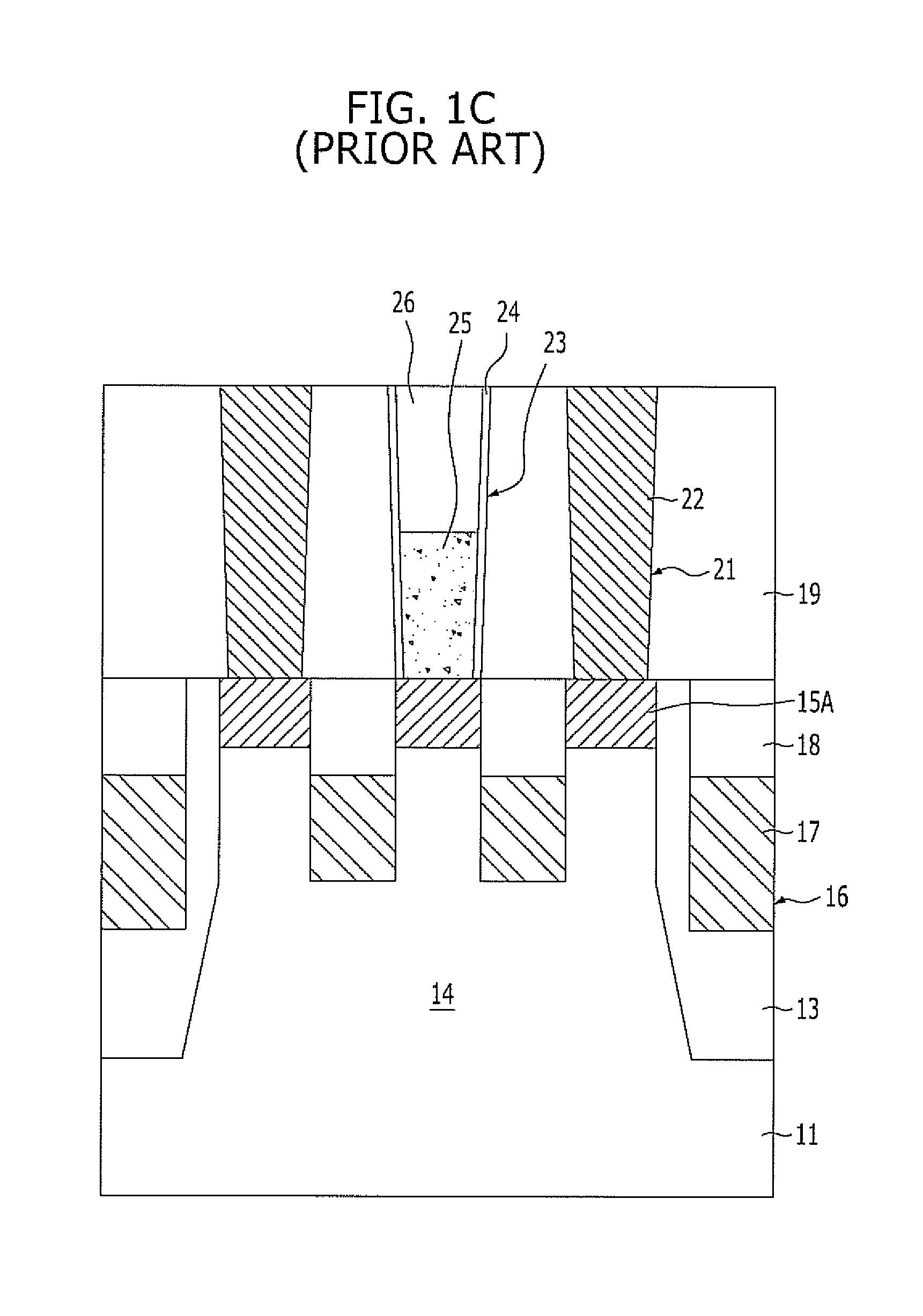
[0025]FIGS. 2A to 2I are cross-sectional views illustrating a method for fabricating a semiconductor device with buried gates in accordance with the present invention.

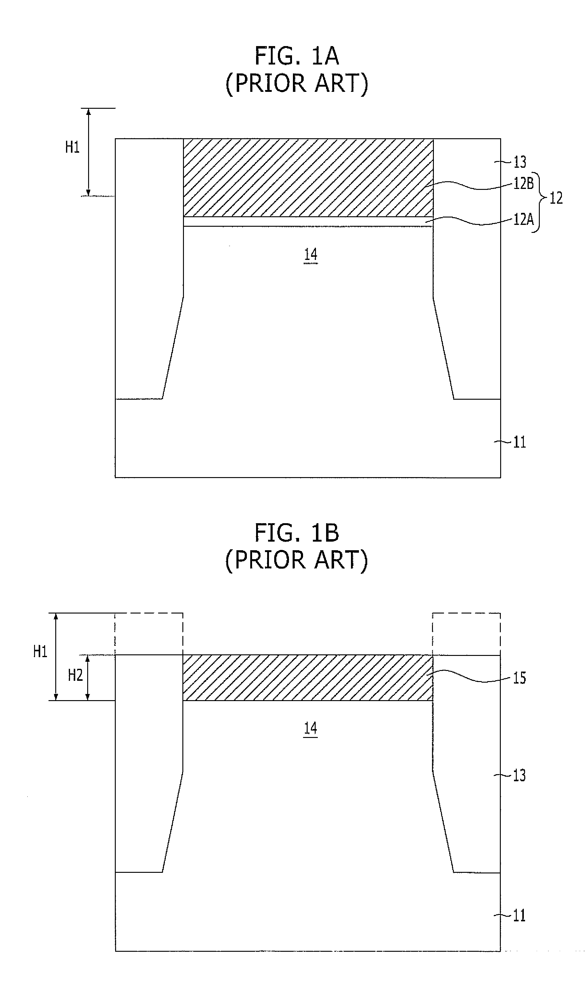
[0026]Referring to FIG. 2A, a hard mask pattern 32 including a pad oxide layer 32A and a hard mask polysilicon layer 32B stacked therein is formed over a substrate 31. The hard mask polysilicon layer 32B substantially functions as an etch barrier, and the pad oxide layer 32A enhances the adhesion between the hard mask polysilicon layer 32B and the substrate 31, e.g., a silicon substrate. Here, when a polysilicon thin film is directly formed over a silicon substrate, peeling of the polysilicon thin film may occur due to poor adhesion between the polysilicon thin film and the silicon substrate.

[0027]The hard mask pattern 32 may be formed to have such a thickness H1 that it may protect active regions 34 from leaning during a subsequent process of forming isolation trenches. Also, the hard mask pattern 32 may be formed to ...

second embodiment

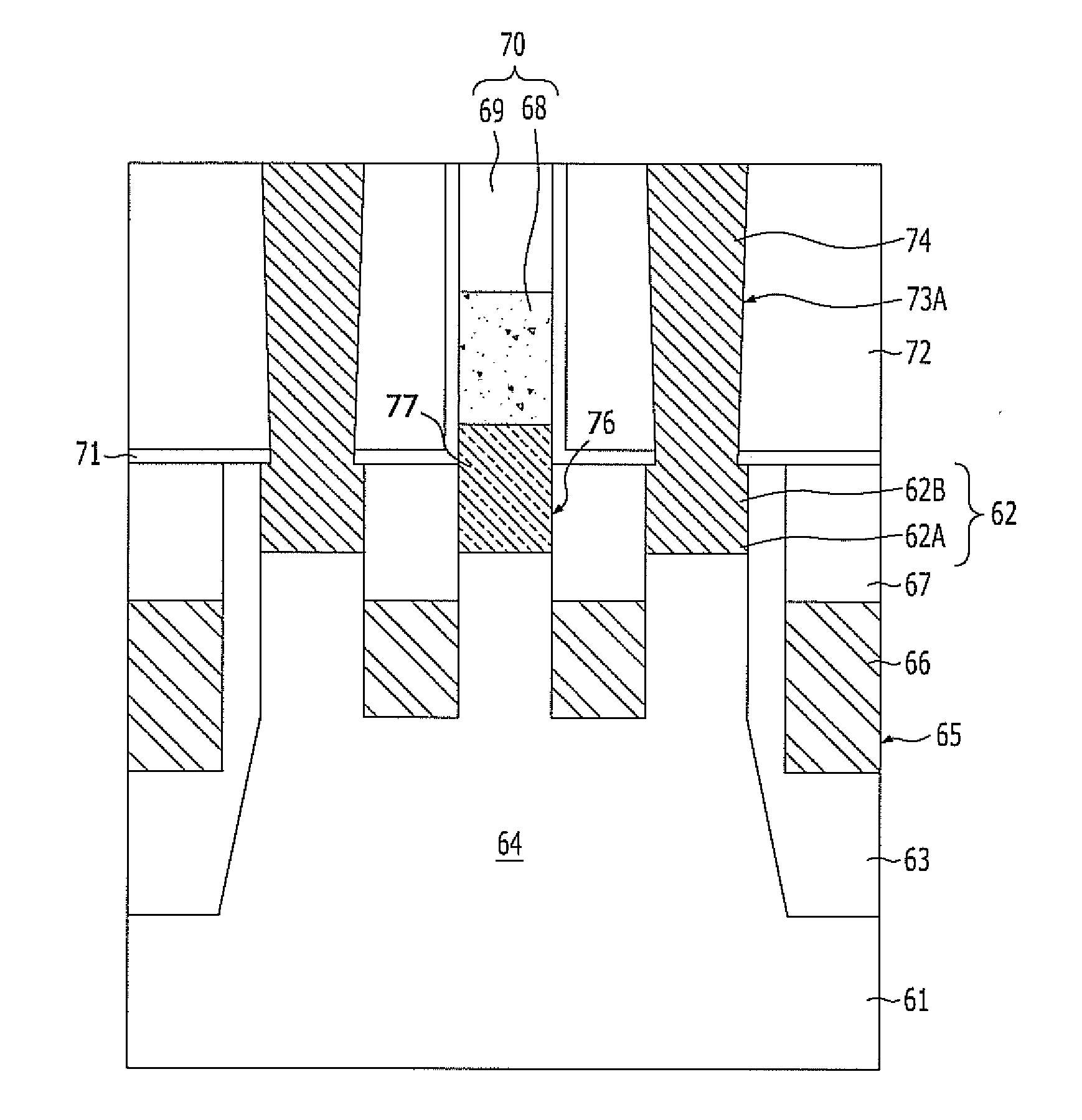
[0052]FIGS. 3A to 3G are cross-sectional views illustrating a method for fabricating a semiconductor device with buried gates in accordance with the present invention.

[0053]As illustrated in FIG. 3A, a first hard mask pattern 62 including a pad oxide layer 62A and a hard mask polysilicon layer 62B stacked therein is formed over a substrate 61. The hard mask polysilicon layer 62B substantially functions as an etch barrier, and the pad oxide layer 62A enhances the adhesion between the hard mask polysilicon layer 62B and the substrate 61, e.g., a silicon substrate. Here, when a polysilicon thin film is directly deposited on the silicon substrate, peeling of the polysilicon thin film may occur due to poor adhesion between the polysilicon thin film and the silicon substrate.

[0054]The first hard mask pattern 62 may be formed to have a thickness H1 to prevent active regions 64 from leaning during a subsequent process of forming isolation trenches. Moreover, the first hard mask pattern 62 m...


PUM


Abstract

A method for fabricating a semiconductor device includes forming a hard mask pattern over a substrate, forming an isolation layer for defining an active region by using the hard mask pattern, forming a buried gate in and across the active region and the isolation layer over the substrate, forming an inter-layer dielectric layer over the substrate, forming a storage node contact hole that exposes the hard mask pattern by selectively etching the inter-layer dielectric layer, extending the storage node contact hole to expose the active region by removing the hard mask pattern exposed under the storage node contact hole, and forming a storage node contact plug that fills the extended storage node contact hole.

Description

CROSS-REFERENCE TO RELATED APPLICATIONS[0001]The present application claims priority of Korean Patent Application No. 10-2010-0128115, filed on Dec. 15, 2010, which is incorporated herein by reference in its entirety.BACKGROUND[0002]1. Field[0003]Exemplary embodiments of the present invention relate to a semiconductor device fabrication technology, and more particularly, to a method for fabricating a semiconductor device with buried gates (BG).[0004]2. Description of the Related Art[0005]As the size of semiconductor devices becomes smaller, it becomes more difficult for the semiconductor devices to have diverse device properties and fabricate such the semiconductor devices. In particular, under the design rule of 40 nm or less, the semiconductor device reaches the technical limitations in forming a gate structure, a bit line structure, and / or a contact structure. Even if the structure is formed, desired device properties may not be obtained. Therefore, the technology of forming buri...

Claims


Application Information

Patent Timeline
IPC IPC(8): H01L21/28
CPCH01L23/485H01L27/10855H01L27/10876H01L27/10885H01L29/1037H01L2924/0002H01L29/4236H01L2924/00H10B12/053H10B12/0335H10B12/482H10B12/34
Inventor SHIN, JONG-HANKIM, KYUNG-BO
Owner SK HYNIX INC
Why Eureka
Try Eureka