Complete recrystallization of semiconductor wafers

Active Publication Date: 2012-06-28
STILE
View PDF4 Cites 3 Cited by
  • Summary
  • Abstract
  • Description
  • Claims
  • Application Information

AI Technical Summary

Benefits of technology

[0018]b) confinement means for

Problems solved by technology

The area with small grains comprises many grain boundaries, which is for example prejudicial in photovoltaics since the created electron-hole pairs may be trapped therein, which decreases the efficiency.
The wafer also comprises many grain boundaries, which causes operating disturbances.
Further, this “ZMR” method, difficult to implement, is very slow, the processing speed ranging from a few millimeters to a few centimeters per minute.
This method is not advantageous since is lengthy and expensive.

Method used


Image

  • Complete recrystallization of semiconductor wafers
  • Complete recrystallization of semiconductor wafers
  • Complete recrystallization of semiconductor wafers

Examples


Embodiment Construction

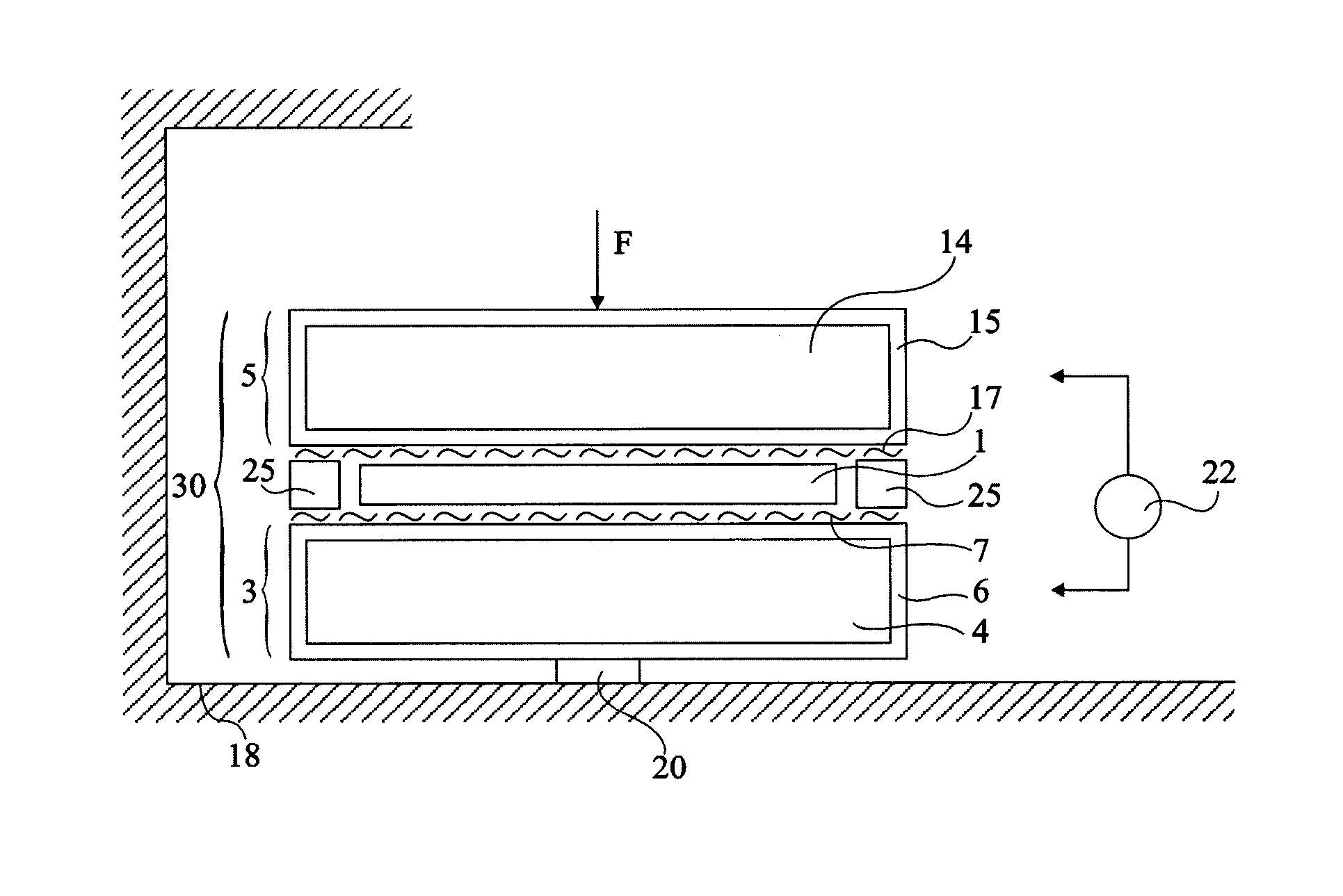
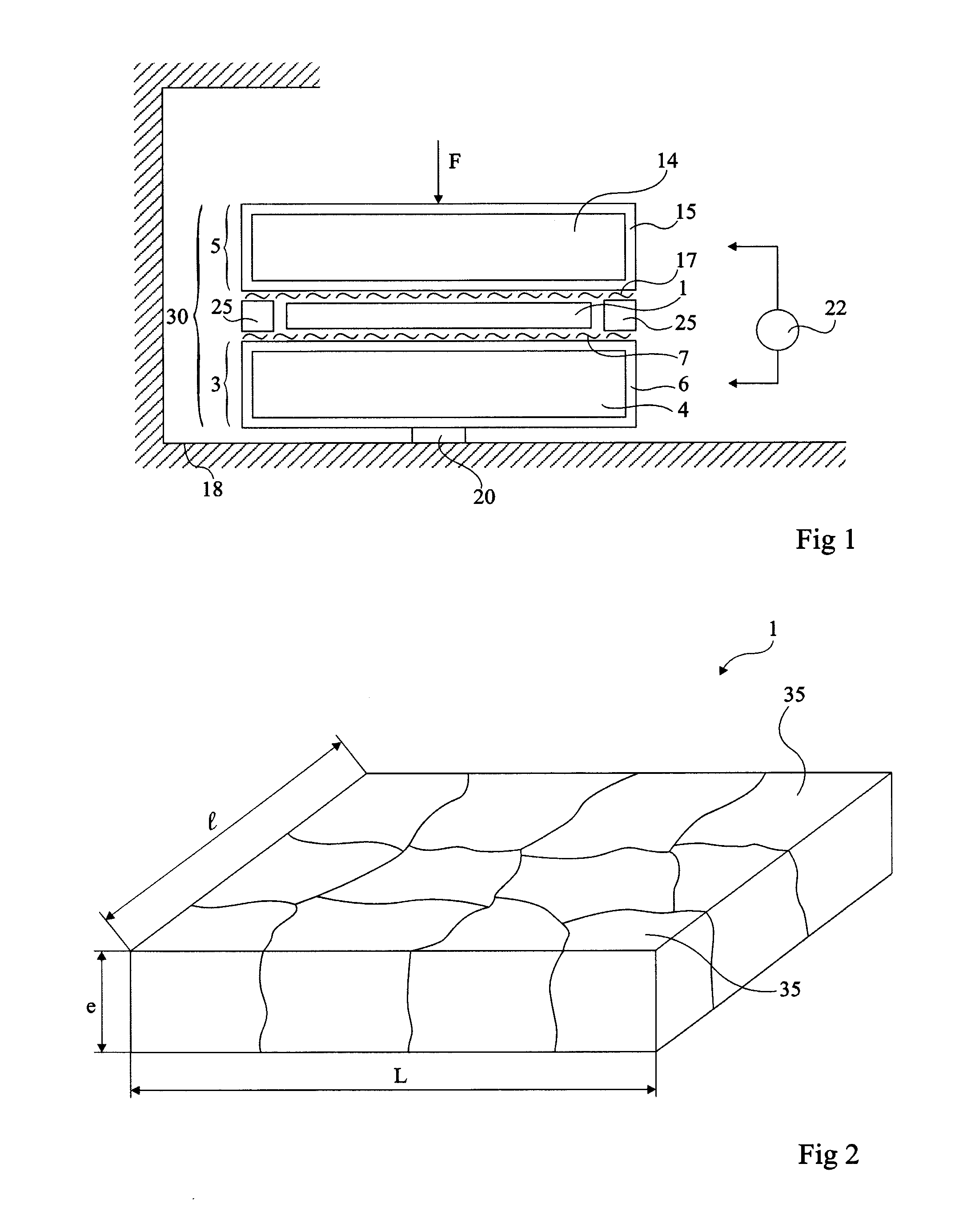
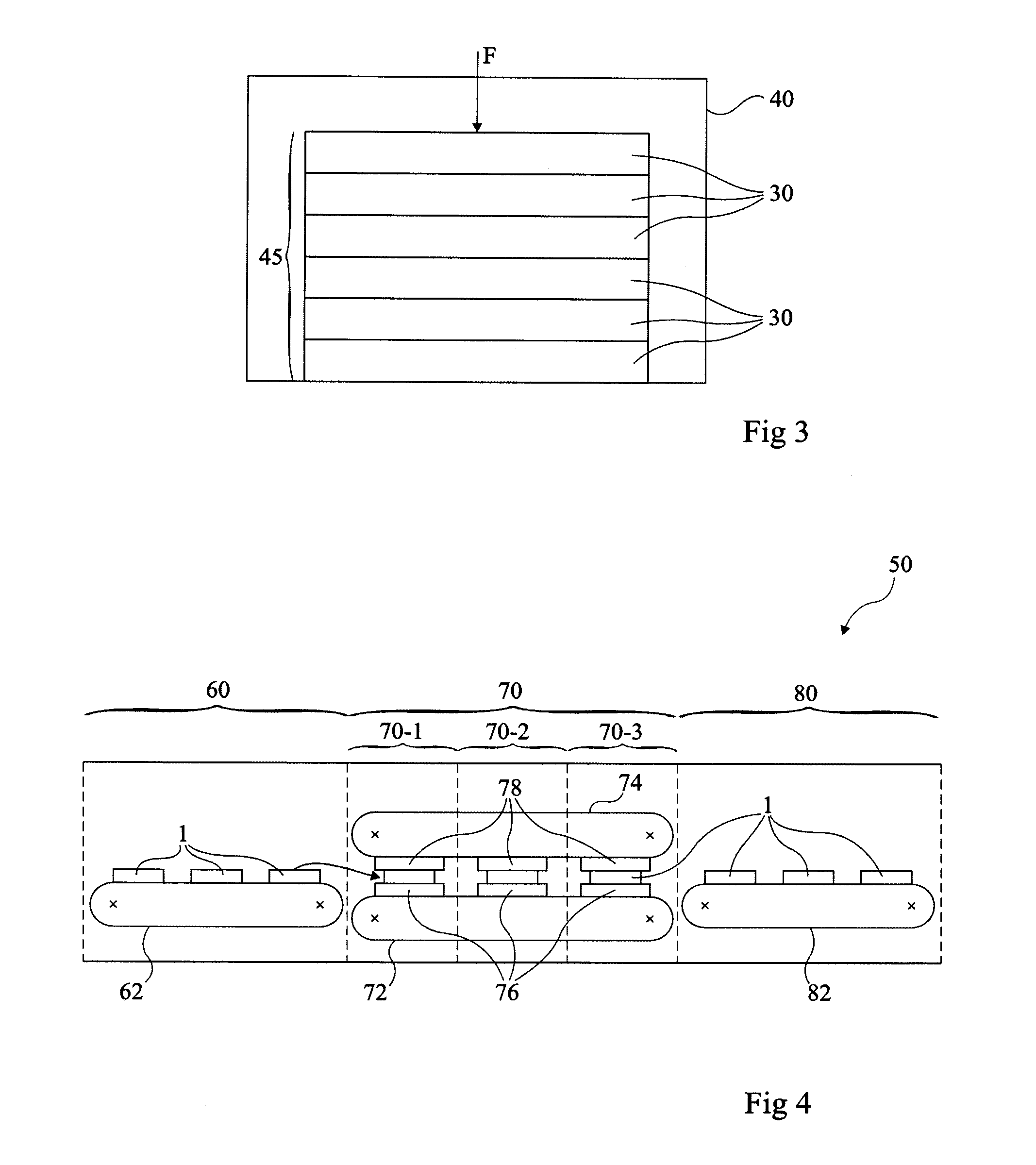
[0033]For clarity, the same elements may have been designated with the same reference numerals in the different drawings and the various drawings are not to scale.

[0034]The principle of the present invention is to fully melt silicon wafers or fully melt the silicon portion of a wafer. “Full melting” means the simultaneous or almost simultaneous melting of the entire silicon volume of the wafer.

[0035]The wafer thickness is not critical. For example, it may range between 100 and 500 micrometers. The thickness may also range up to several millimeters, for example, in photovoltaic applications, or more when, for example, the wafer comprises a support which is not made of silicon.

[0036]After the full melting of silicon, the wafer is recrystallized, and macroscopic silicon grains having a large surface size in all directions then form. If the wafer is only made of silicon, the grains are through, that is, they span from one surface of the wafer to the other. The recrystallization is very ...


PUM


Abstract

The instant disclosure relates to a device and method for recrystallising a silicon wafer or a wafer comprising at least one silicon layer. The silicon wafer or the at least one silicon layer of the wafer is totally molten.

Description

FIELD OF THE INVENTION[0001]The present invention relates to semiconductor wafers intended for various fields of electronics, such as microelectronics, optoelectronics, photovoltaics, etc.DISCUSSION OF PRIOR ART[0002]In unpublished French patent application No. 09 / 52110 of the same inventor, entitled “Structure électronique à couche épitaxiée sur silicium fritté”, the applicant describes a method comprising a step of surface recrystallization of silicon wafers obtained by sintering of silicon powders. Such wafers, after partial recrystallization, comprise an area with large grains and an area with small grains. The area with small grains comprises many grain boundaries, which is for example prejudicial in photovoltaics since the created electron-hole pairs may be trapped therein, which decreases the efficiency.[0003]This same French patent application discusses a zone melting method (ZMR), in which a small moving area is melted across the entire thickness of the wafer. This method g...

Claims


Application Information

Patent Timeline
IPC IPC(8): H01L21/66F27B9/00
CPCF27D3/0084H01L21/02532H01L21/02667H01L21/67098C30B1/12C30B1/02C30B29/06C30B35/00C30B35/002H01L21/6776
Inventor STRABONI, ALAIN
Owner STILE
Why Eureka
Try Eureka