Polishing apparatus and polishing method

a technology of polishing apparatus and polishing method, which is applied in the direction of manufacturing tools, lapping machines, semiconductor/solid-state device testing/measurement, etc., can solve the problems of insufficient data, difficult to obtain accurate film thickness in the peripheral portion, and inability to provide accurate film thickness. , to achieve the effect of high-quality film thickness

Active Publication Date: 2012-06-28
EBARA CORP
View PDF12 Cites 29 Cited by
  • Summary
  • Abstract
  • Description
  • Claims
  • Application Information

AI Technical Summary

Benefits of technology

[0024]According to the present invention, the tip of the second optical head moves along the peripheral portion of the substrate with the rotation of the polishing table. Therefore, the number of measuring points on the peripheral portion is increased, so that more highly accurate film thickness can be obtained. As a result, a highly-accurate film-thickness profile (i.e., a film-thickness distribution along the radial direction of the substrate) can be created during polishing, and a desired film-thickness profile can be obtained based on the created film-thickness profile.

Problems solved by technology

However, in the conventional CMP apparatus, an accurate film thickness cannot be obtained in the peripheral portion of the substrate because of the smaller number of measuring points on this potion.
However, as described above, it is difficult to obtain an accurate film thickness in the peripheral portion because of the smaller number of measuring points on this portion.
This is because the small number of measuring points in the peripheral portion cannot provide sufficient data for the smoothing.
As described above, it is difficult to obtain highly-accurate film-thickness data in the peripheral portion of the substrate, and consequently a highly-accurate film-thickness profile of the substrate cannot be obtained during polishing.
As a result, it has been difficult to obtain a desired film-thickness profile through feedback of the film-thickness profile to the polishing load.

Method used


Image

  • Polishing apparatus and polishing method
  • Polishing apparatus and polishing method
  • Polishing apparatus and polishing method

Examples


Embodiment Construction

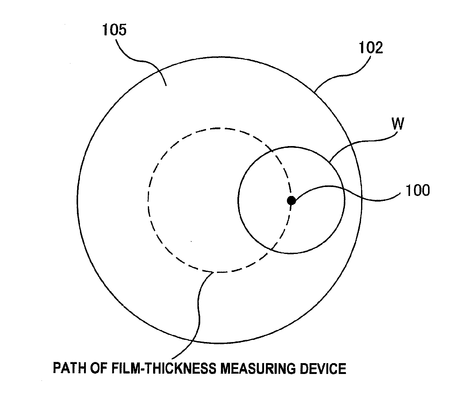
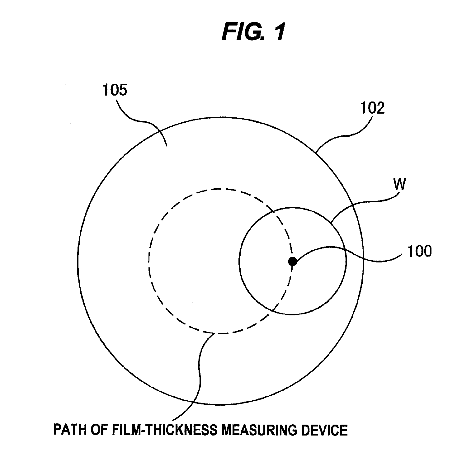
[0051]Embodiments of the present invention will be described below with reference to the drawings. FIG. 4A is a schematic view showing the principle of determining a film thickness based on a spectrum of a reflected light from a substrate, and FIG. 4B is a plan view showing a positional relationship between the substrate and a polishing table. As shown in FIG. 4A, a substrate W, to be polished, has an underlying layer (e.g., a silicon layer) and a film (e.g., a dielectric film, such as SiO2, having a property of light permeability) formed on the underlying layer. A surface of the substrate W is pressed against a polishing pad 22 on a rotating polishing table 20, so that the film of the substrate W is polished by sliding contact with the polishing pad 22.

[0052]A light-applying unit 11 and a light-receiving unit 12 are arranged so as to face the surface of the substrate W. The light-applying unit 11 is coupled to a light source 16, and light emitted by the light source 16 is directed ...


PUM


Abstract

A polishing apparatus for polishing a substrate is provided. The polishing apparatus includes: a polishing table holding a polishing pad; a top ring configured to press the substrate against the polishing pad; first and second optical heads each configured to apply the light to the substrate and to receive reflected light from the substrate; spectroscopes each configured to measure at each wavelength an intensity of the reflected light received; and a processor configured to produce a spectrum indicating a relationship between intensity and wavelength of the reflected light. The first optical head is arranged so as to face a center of the substrate, and the second optical head is arranged so as to face a peripheral portion of the substrate.

Description

BACKGROUND OF THE INVENTION[0001]1. Field of the Invention[0002]The present invention relates to a polishing apparatus for polishing a surface of a substrate, such as a semiconductor wafer, and more specifically to a polishing apparatus and a polishing method which obtain a film-thickness distribution over the entire substrate surface including a central portion and a peripheral portion thereof during polishing of the substrate and control a load on the substrate based on the film-thickness distribution.[0003]2. Description of the Related Art[0004]CMP (chemical mechanical polishing) apparatus is widely known as equipment for polishing a surface of a substrate, such as a semiconductor wafer. This CMP apparatus polishes the surface of the substrate by pressing the substrate against a polishing pad on a rotating polishing table while supplying a polishing liquid onto the polishing pad. The CMP apparatus typically has a film-thickness measuring device for measuring a film thickness or a...

Claims


Application Information

Patent Timeline
Patent Type & Authority Applications(United States)
IPC IPC(8): B24B49/00
CPCB24B37/005B24B49/12B24B37/04B24B37/013B24B37/042B24B37/10B24B37/205B24B37/26B24B37/12B24B37/30H01L21/02013H01L21/302H01L21/304H01L21/31053H01L21/67075H01L21/67092H01L21/67253H01L21/68721H01L22/26
Inventor KOBATA, ITSUKIKOBAYASHI, YOICHIONO, KATSUTOSHIKINOSHITA, MASAKIKIMBA, TOSHIFUMI
Owner EBARA CORP
Why Eureka
Try Eureka