Laminate type electronic component and manufacturing method therefor

a technology of electronic components and manufacturing methods, which is applied in the direction of fixed capacitor details, generators/motors, fixed capacitors, etc., can solve the problems of insufficient ensuring of capacitance, inability to reduce the effective volume of ensuring capacitance, and defects in plating films that are easy to blister or bulge, so as to improve alignment accuracy and facilitate growth

Active Publication Date: 2012-07-05
MURATA MFG CO LTD
View PDF7 Cites 3 Cited by
  • Summary
  • Abstract
  • Description
  • Claims
  • Application Information

AI Technical Summary

Benefits of technology

[0026]In addition, the open ends of the cuts, which preferably have a width dimension of about 10 μm or less, for example, make it easier to grow the upper plating films by plating so as to form bridges over the slits of the base plating films, in the case of forming the upper plating films on the plating films to fill the slits of the plating films.
[0027]As described above, when the external electrodes further include the upper plating films formed on the base plating films to fill the slits, the respective surfaces of the external electrodes will not be divided, but provided by uniform films. Thus, the mountability of the laminate type electronic component, for example, by reflow soldering, in particular, the alignment accuracy can be improved.
[0028]The above and other elements, features, steps, characteristics and advantages of the present invention will become more apparent from the following detailed description of the preferred embodiments with reference to the attached drawings.

Problems solved by technology

Therefore, in order to limit the dimensions of the laminate type electronic component up to certain specifications, there is undesirably a need to reduce the effective volume for ensuring a capacitance, because there is a need to ensure the volume for the paste electrode layers.
In addition, the ingress of moisture other than the plating solution into the component main body may occur.
However, the path for releasing moisture in the component main body is covered with the plating films after the plating step, thus not only interfering with the release of moisture, but also causing blisters or bulge defects in the plating films.

Method used


Image

  • Laminate type electronic component and manufacturing method therefor
  • Laminate type electronic component and manufacturing method therefor
  • Laminate type electronic component and manufacturing method therefor

Examples


Embodiment Construction

[0035]First, as shown in FIG. 6, a laminate type electronic component 1 according to a preferred embodiment of the present invention includes a component main body 2, and first and second external electrodes 3 and 4 are disposed on the outer surface of the component main body 2.

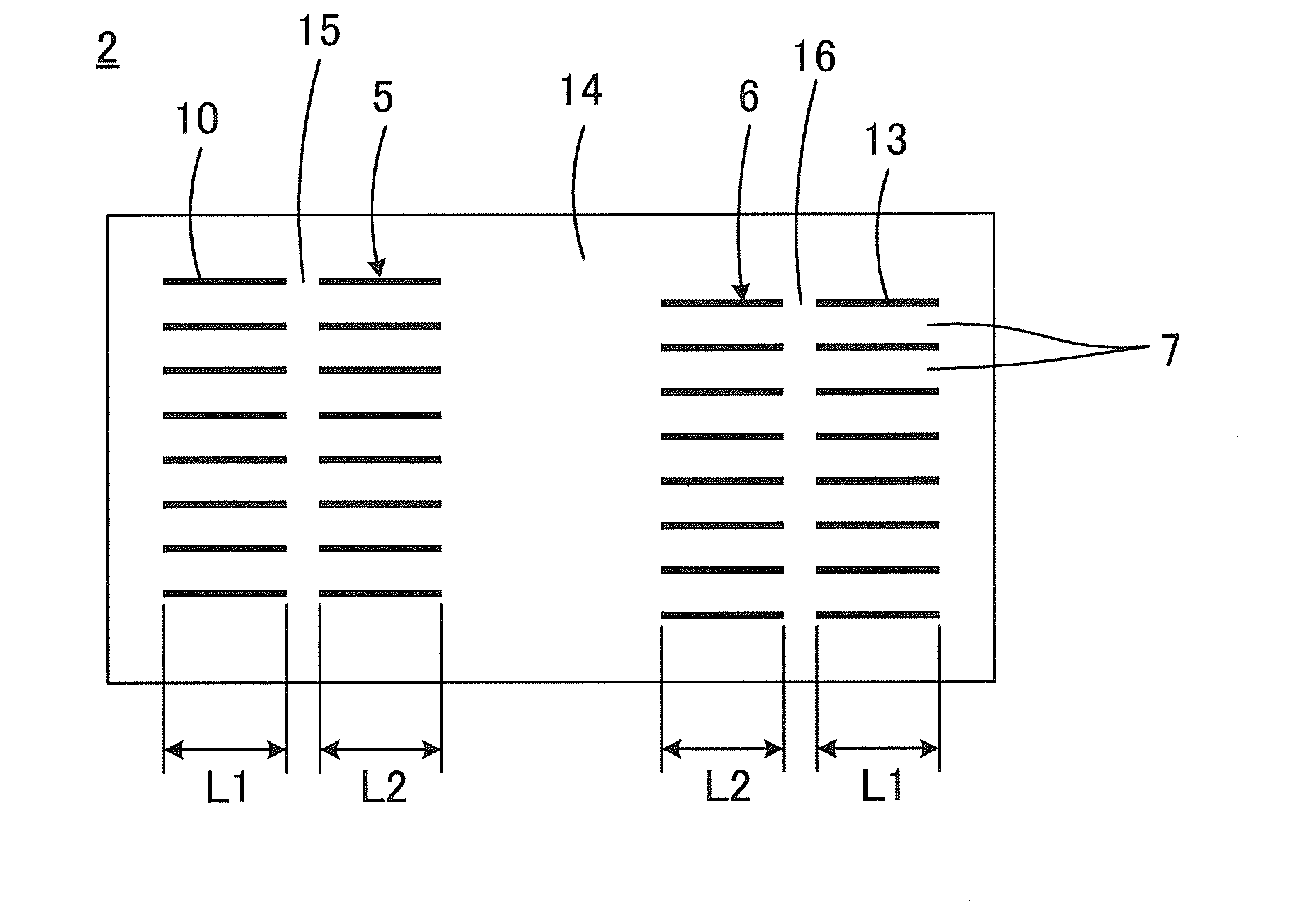
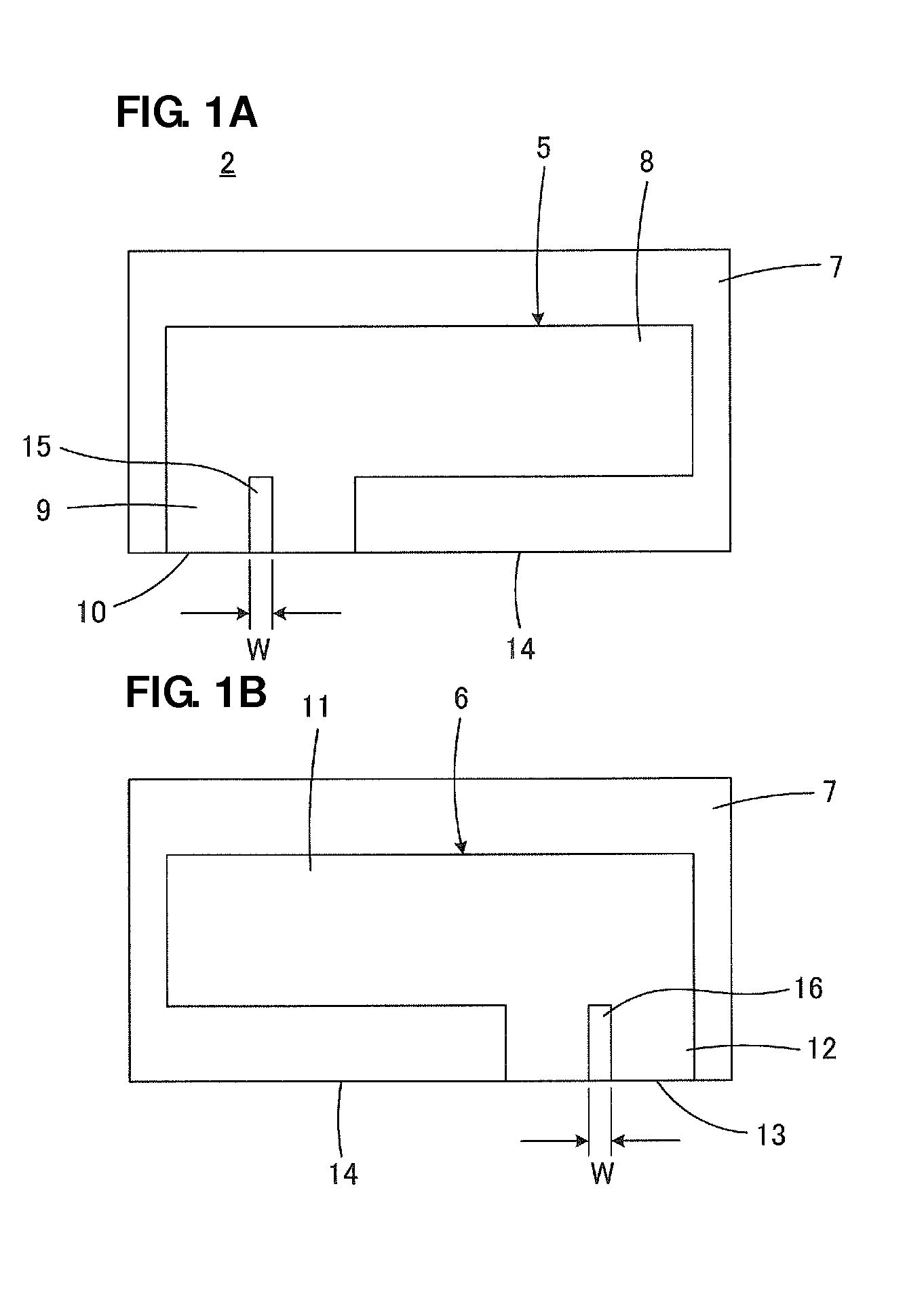
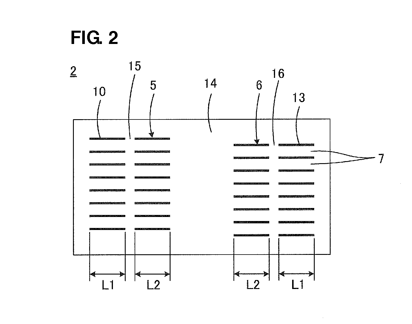
[0036]The component main body 2 includes a plurality of first internal electrodes 5 and a plurality of second internal electrodes 6 disposed therein as shown in FIGS. 1 and 2. More specifically, the component main body 2 has a stacked structure including a plurality of stacked functional material layers 7, and the first and second internal electrodes 5 and 6 are arranged along the interfaces between the functional material layers 7. The first internal electrodes 5 and the second internal electrodes 6 are arranged alternately in the stacking direction. The internal electrodes 5 and 6 include, for example, nickel as their main constituent.

[0037]When the laminate type electronic component 1 constitutes a laminat...


PUM

PropertyMeasurementUnit
temperatureaaaaaaaaaa
widthaaaaaaaaaa

Abstract

In a method of manufacturing a laminate type electronic component, when a heat treatment is carried out after plating films, which at least partially define external electrodes, are formed by growing plated depositions deposited on exposed ends of a plurality of internal electrodes in a component main body, the presence of the plating films may not only interfere with moisture release, but may also cause blisters or bulge defects in the plating films, while moisture such as a plating solution in the component main body is removed by evaporation. To avoid such problems, cuts to divide exposed ends into multiple sections are formed in extending sections of internal electrodes. Thus, plating films include slits extending in the stacking direction at locations corresponding to positions of the cuts.

Description

BACKGROUND OF THE INVENTION[0001]1. Field of the Invention[0002]The present invention relates to a laminate type electronic component and a method for manufacturing the laminate type electronic component, and more particularly, relates to a laminate type electronic component including an external electrode formed directly by plating such that the external electrode is connected electrically to a plurality of internal electrodes, and a method for manufacturing the laminate type electronic component.[0003]2. Description of the Related Art[0004]Laminate type electronic components typified by laminated ceramic capacitors are, in general, provided with a component main body which has a stacked structure including, for example, a plurality of stacked functional material layers composed of a dielectric ceramic, and a plurality of layered internal electrodes formed along the interfaces between the functional material layers. The respective ends of the plurality of internal electrodes are ex...

Claims


Application Information

Patent Timeline
Patent Type & Authority Applications(United States)
IPC IPC(8): H01L41/00H01F5/00B05D3/02H01C7/10B05D5/12H01G4/12H01C7/13H01G4/232H01G4/30
CPCH01G4/012H01G4/30H01G4/232
Inventor SARUBAN, MASAHITOOGAWA, MAKOTOOGAWA, WATARUMOTOKI, AKIHIROTAKEUCHI, SYUNSUKEYAMAMOTO, YOJI
Owner MURATA MFG CO LTD
Why Eureka
Try Eureka