Wafer carrier with selective control of emissivity

Inactive Publication Date: 2012-07-05
VEECO INSTR
View PDF9 Cites 18 Cited by
  • Summary
  • Abstract
  • Description
  • Claims
  • Application Information

AI Technical Summary

Benefits of technology

[0010]One aspect of the present invention provides a wafer carrier. A wafer carrier according to this aspect of the invention desirably includes a body having an outer surface. Preferably, the outer surface of the body includes oppositely-facing top and bottom surfaces and an edge surface extending between the top and bottom surfaces. The top surface prefera

Problems solved by technology

Minor variations in composition of the reactive gases and in the temperature of the wafer surfaces cause undesired variations in the properties of the resulting semiconductor devices.

Method used


Image

  • Wafer carrier with selective control of emissivity
  • Wafer carrier with selective control of emissivity
  • Wafer carrier with selective control of emissivity

Examples


Embodiment Construction

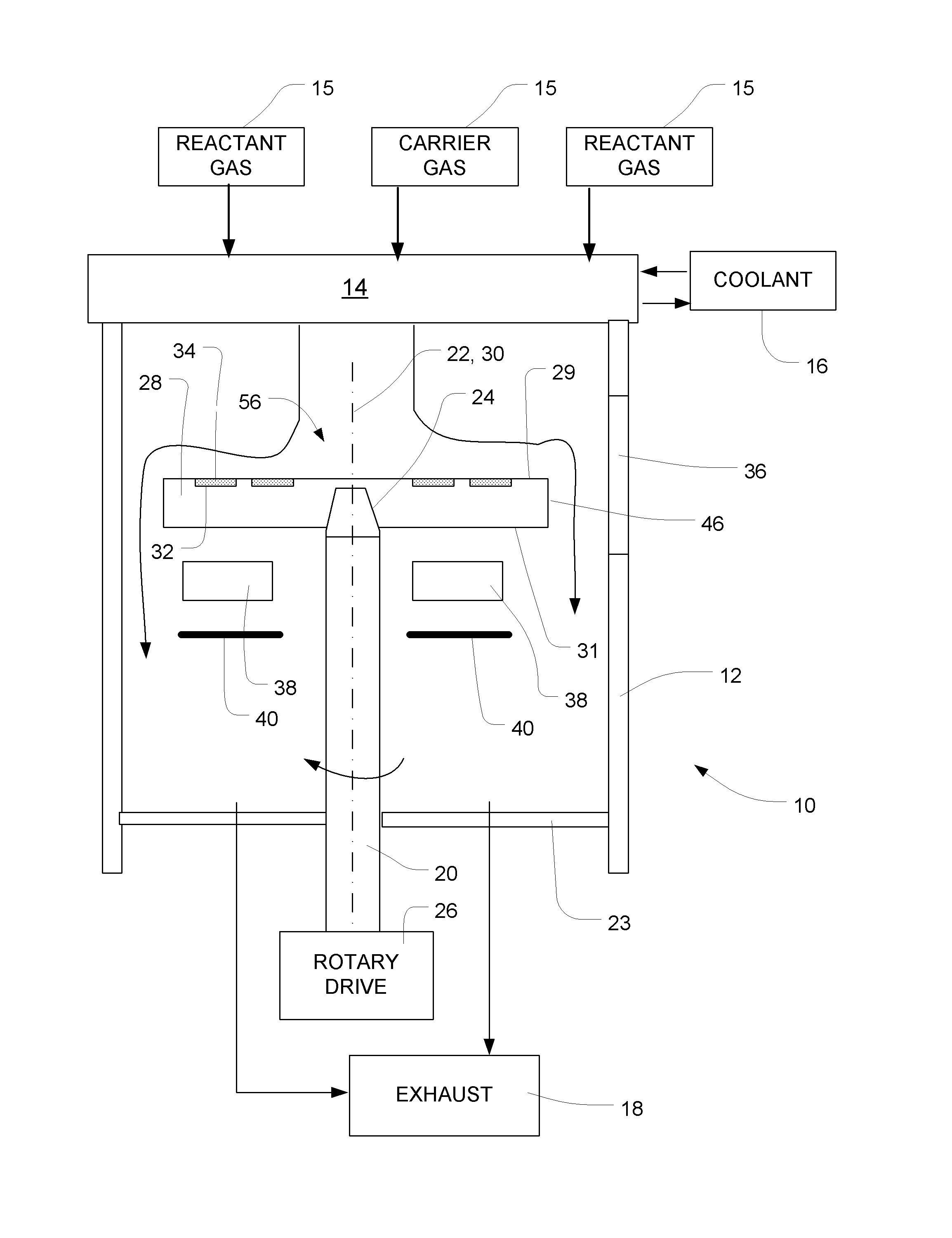
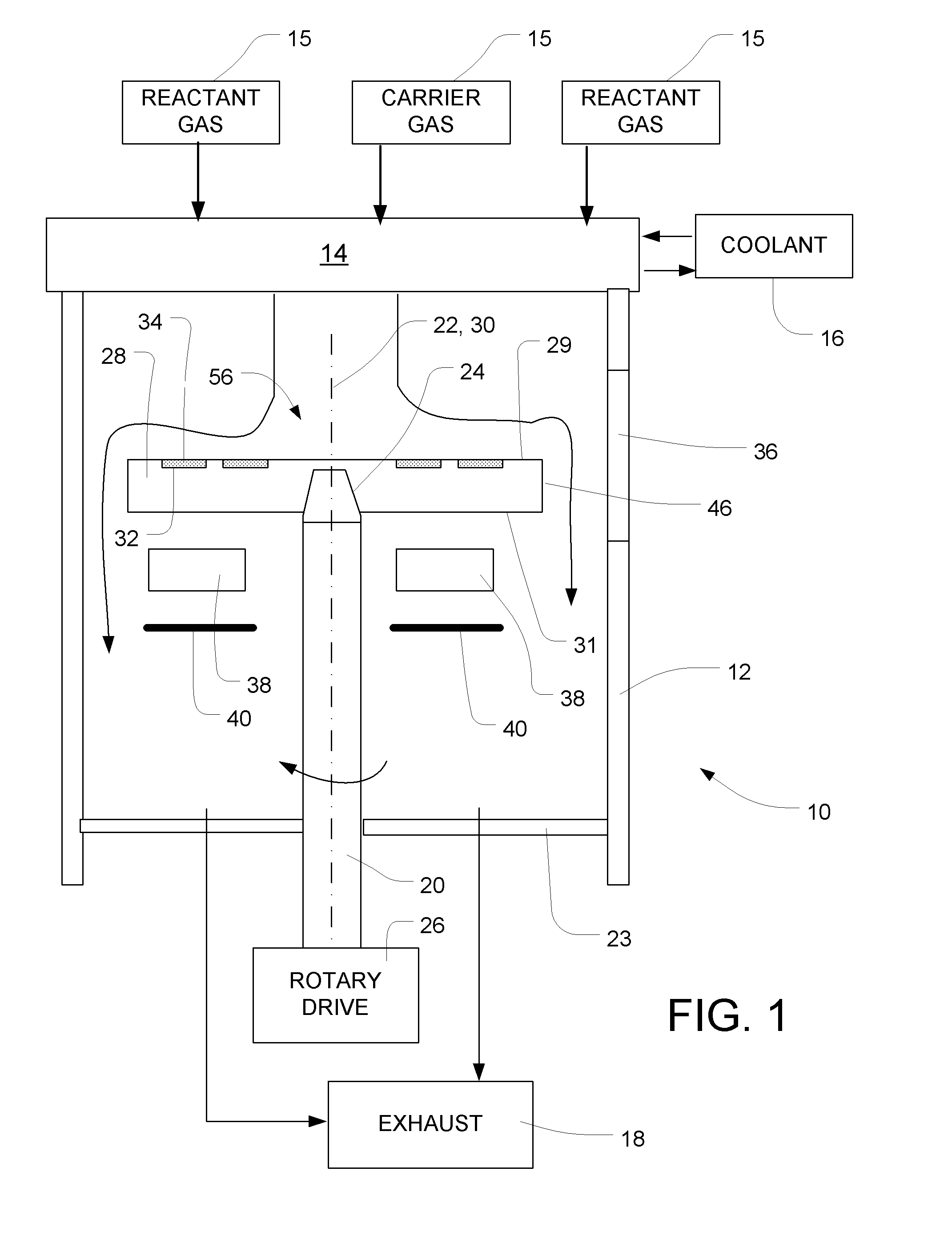
[0024]Referring to FIG. 1, a chemical vapor deposition apparatus 10 in accordance with one embodiment of the invention includes a reaction chamber 12 having a gas distribution element 14 arranged at one end of the chamber 12. The end of the chamber 12 having the gas distribution element 14 is referred to herein as the “top” end of the chamber 12. This end of the chamber typically, but not necessarily, is disposed at the top of the chamber in the normal gravitational frame of reference. Thus, the downward direction as used herein refers to the direction away from the gas distribution element 14; whereas the upward direction refers to the direction within the chamber, toward the gas distribution element 14, regardless of whether these directions are aligned with the gravitational upward and downward directions. Similarly, the “top” and “bottom” surfaces of elements are described herein with reference to the frame of reference of chamber 12 and element 14.

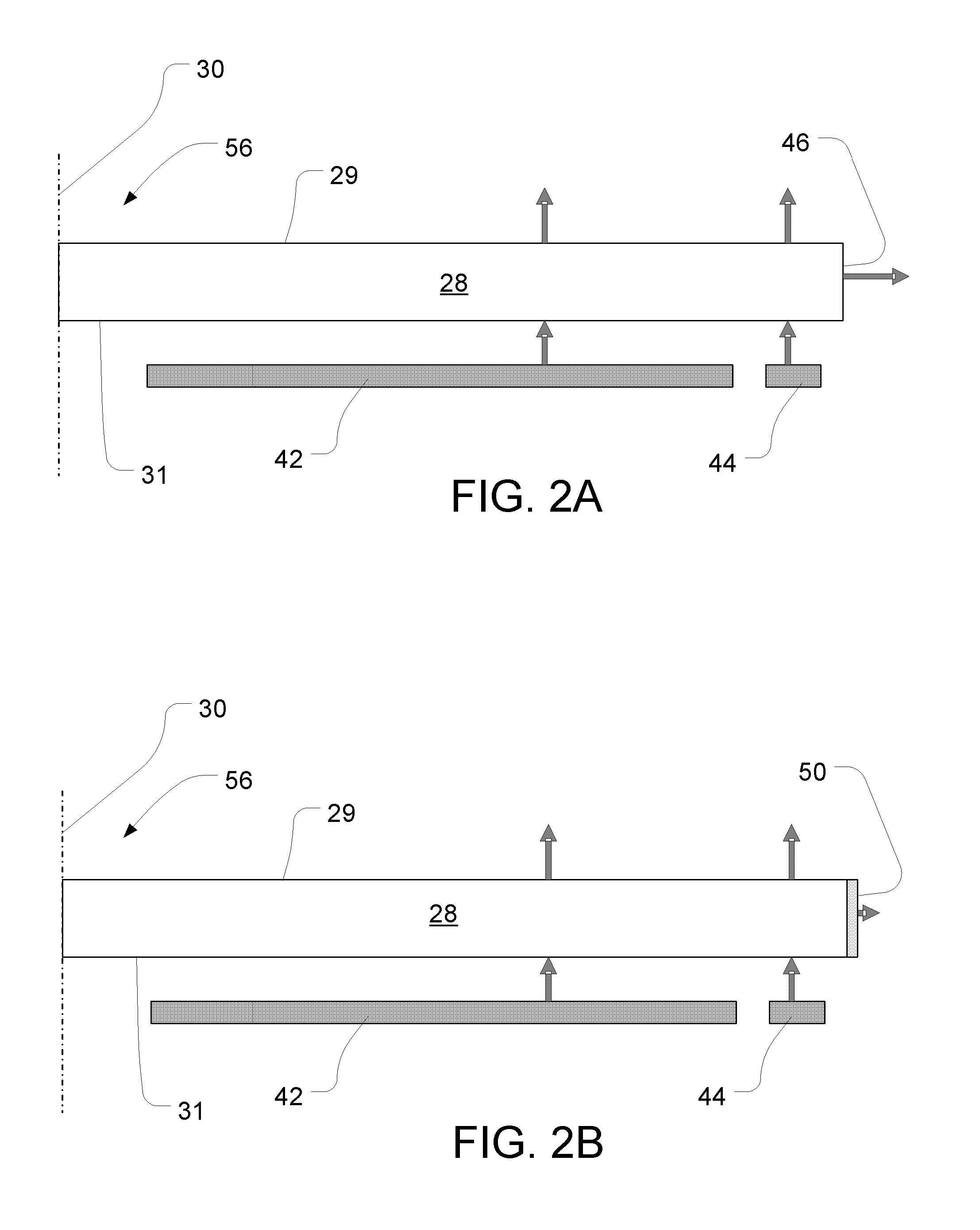
[0025]The gas distribution ele...


PUM

PropertyMeasurementUnit
Temperatureaaaaaaaaaa
Shapeaaaaaaaaaa

Abstract

A wafer carrier for use in a chemical vapor deposition apparatus includes at least one region on its outer surface having a substantially different (e.g., lower) emissivity than other regions on the outer surface. The modified emissivity region may be located on the outer edge, the top surface, and / or the bottom surface of the carrier. The region may be associated with one or more wafer pockets of the wafer carrier. The modified emissivity region may be shaped and sized so as to modify the heat transmission through the region, and thereby increase the temperature uniformity across portions of the top surface of the wafer carrier or across individual wafers. The modified emissivity region may be provided by a coating on the outer surface of the wafer carrier.

Description

BACKGROUND OF THE INVENTION[0001]The present invention relates to wafer processing apparatus, to wafer carriers for use in such processing apparatus, and to methods of controlling the emissivity of such wafer carriers.[0002]Many semiconductor devices are formed by processes performed on a substrate. The substrate typically is a slab of a crystalline material, commonly referred to as a “wafer.” One common process for forming devices on a wafer is epitaxial growth.[0003]For example, devices formed from compound semiconductors such as III-V semiconductors typically are formed by growing successive layers of a compound semiconductor using metal organic chemical vapor deposition or “MOCVD.” In this process, the wafers are exposed to a combination of gases, typically including a metal organic compound as a source of a group III metal, and also including a source of a group V element which flow over the surface of the wafer while the wafer is maintained at an elevated temperature. Typicall...

Claims


Application Information

Patent Timeline
IPC IPC(8): C23C16/46C23C16/458
CPCH01L21/68771H01L21/68757
Inventor VOLF, BORISWEI, GUANGHUARASHKOVSKY, YULIY
Owner VEECO INSTR
Why Eureka
Try Eureka