Film containing nested micro trap structure and preparation method thereof

A nesting and trapping technology, applied in ion implantation plating, metal material coating process, coating, etc., can solve problems such as high-power microwave system not working normally, component surface erosion, affecting equipment performance, etc.

Inactive Publication Date: 2021-12-03
XI AN JIAOTONG UNIV +1
View PDF8 Cites 0 Cited by
  • Summary
  • Abstract
  • Description
  • Claims
  • Application Information

AI Technical Summary

Problems solved by technology

The secondary electron multiplication effect can lead to the gradual increase of the standing wave ratio of the microwave transmission system, the increase of the reflected power, and the increase of the noise level, resulting in the failure of the high-power microwave system to work normally; micro-discharge can also cause intracavity tuning, parameter coupling, waveguide Fluctuations in loss and phase constants, etc., generate harmonics that cause out-of-band interference and passive intermodulation products, and cause erosion on the surface of components, etc.
However, the single method of changing the surface morphology of the material has a non-negligible impact on the performance of the material itself. Although it plays a certain role in the suppression of secondary electrons, it affects the performance of the device in other ways.

Method used


Image

  • Film containing nested micro trap structure and preparation method thereof
  • Film containing nested micro trap structure and preparation method thereof
  • Film containing nested micro trap structure and preparation method thereof

Examples


Embodiment

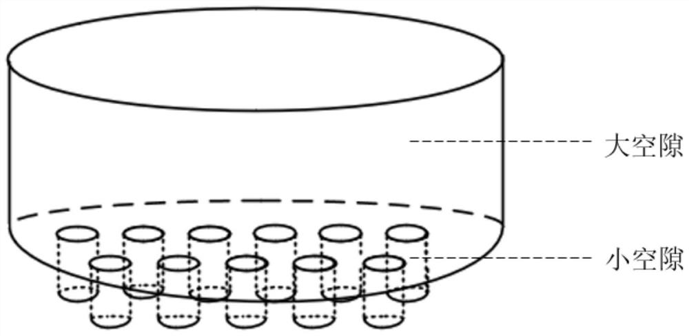
[0036] In order to obtain a high-quality secondary electron suppression film with a nested micro-trap structure, we choose C material as the lower material film and Ag material as the upper material film. The reason for choosing these two materials is due to the atomic radius of C Smaller, the covalent radius is also smaller when forming a thin film, and the Ag atom has a larger atomic radius than the C atom, and the covalent radius is also larger when forming a thin film, so that it is easier to make the lower layer with a smaller atomic gap when coating The material film and the upper material film with a larger atomic gap form a nested trap structure with higher quality. For the substrate, we choose the aluminum alloy silver-plated material commonly used in space microwave materials.

[0037] A method for preparing a thin film containing a nested micro-trap structure, specifically comprising the following steps:

[0038] Step 1: Cleaning, an aluminum alloy silver-plated su...


PUM


Abstract

The invention discloses a film containing a nested micro trap structure and a preparation method thereof. The film comprises a lower-layer material film, an upper-layer material film and a substrate, wherein the lower-layer material film is arranged on the substrate, and the upper-layer material film is arranged on the lower-layer material film; the atomic gap of the lower-layer material film is smaller than the atomic gap of the upper-layer material film, and the atomic gap of the lower-layer material film is nested into the atomic gap of the upper-layer material film to form a nested micro-trap structure. According to the invention, the film with the nested micro-trap structure is grown by using the magnetron sputtering technology, the upper and lower layers of films with different densities are formed by controlling the sputtering power, the lower-layer film is small in sputtering power, large in material density and small in atomic spacing, and small gaps exist between atoms; the upper-layer film is high in sputtering power, low in material density and large in atom spacing, large gaps exist among atoms, and the large gaps and the small gaps of the upper layer and the lower layer form a nested micro trap structure.

Description

technical field [0001] The invention belongs to the technical field of secondary electron emission suppression, and in particular relates to a thin film containing a nested micro-trap structure and a preparation method thereof. Background technique [0002] my country's spacecraft payload urgently needs to develop towards integration and high power. However, in the harsh space environment, it will also lead to the intensification of some special effects in space. The micro-discharge effect of space high-power microwave components is the first problem. The space micro-discharge effect, also known as the secondary electron multiplication effect, refers to the resonant discharge phenomenon that occurs when high-power microwave components transmit high-power microwave signals at a pressure of 1×10⁻³Pa or lower. The micro-discharge effect is a very important factor affecting the reliability of aerospace electronic equipment. Due to the rapid development of space electronic equip...

Claims


Application Information

Patent Timeline
Patent Type & Authority Applications(China)
IPC IPC(8): C23C14/06C23C14/16C23C14/35
CPCC23C14/0605C23C14/165C23C14/35
Inventor 胡忠强赵亚楠朱媛媛刘明何鋆胡天存张毅崔万照
Owner XI AN JIAOTONG UNIV
Why Eureka
Try Eureka