Input device and associated method

a technology of input device and input method, which is applied in the direction of input/output process of data processing, instruments, electric digital data processing, etc., can solve the problems of reducing the accuracy of users, self-sustaining avalanche, and fundamental limitations of touch screen technology in the accuracy which users can achieve, so as to provide mouse style control and accuracy

Active Publication Date: 2012-08-02
STMICROELECTRONICS (RES & DEV) LTD
View PDF15 Cites 24 Cited by
  • Summary
  • Abstract
  • Description
  • Claims
  • Application Information

AI Technical Summary

Benefits of technology

[0030]The proposed invention is able to locate an object within an area outside of the device without it being necessary for the object to contact a solid surface and can be positioned so as not to imply 1:1 location mapping whilst using no additional device space. Because of this, the system is able to provide mouse style control and accuracy for parent devices without the space requirements of a track pad or additional peripherals such as a mouse or stylus.

Problems solved by technology

The high reverse bias voltage generates a sufficient magnitude of electric field such that a single charge carrier introduced into the depletion layer of the device can cause a self-sustaining avalanche via impact ionisation.
Touch screen technology is fundamentally limited in the accuracy which a user can achieve.
For example, the user's finger, stylus, or other touching object will obstruct the user's view of the display thereby reducing the accuracy which a user can achieve.
In addition, the mapping between a touch sensitive user interface and a device display for intuitive user operation may use a 1:1 location mapping between a touch sensitive user interface and a device display—this can result in a user interface which is too small to operate accurately.
However, this uses additional area on the device, rendering it impractical for mobile devices (such as, but not limited to, mobile phones, laptops and tablet PCs) where space is often at a premium.
An additional problem is that the cost of a touch screen and a track pad increase in proportion to their area.
However these have not proved successful for a number of reasons.
In particular although conventional 3D cameras are able to produce a depth map of a scene, they are expensive, bulky, have high power consumption and require very high data bandwidth operating at the high frame rates used for low-latency response times essential for user perception of system performance.
The Microsoft Kinect™ system uses light matrix scattering detection techniques to produce a depth map of a scene, but requires heavy data processing, is physically large, and can only achieve a 30 Hz frame rate which compromises accuracy of object tracking.
Projection keyboards utilise a similar method of detection but are also limited in frame rate, e.g. Canestra™ Electronic Perception Technology (EPT) keyboard can sense “up to 400 characters per minute” (6.667 per second).
As a result of these issues, virtual projected keyboards have been expensive, limited to operating in an imaging mode, have higher bandwidth and processing requirements, and limited due to the need to project onto a hard, non-reflective surface to work.

Method used


Image

  • Input device and associated method
  • Input device and associated method
  • Input device and associated method

Examples


Embodiment Construction

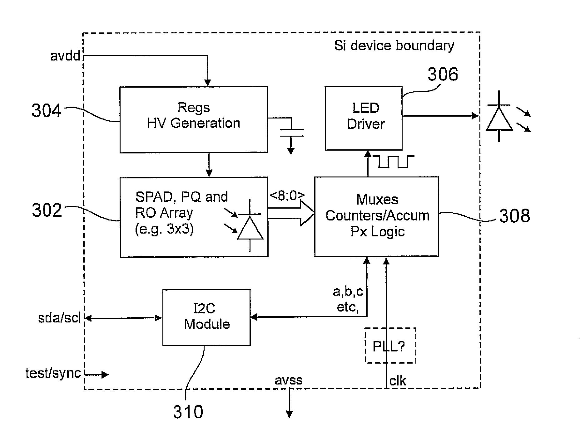
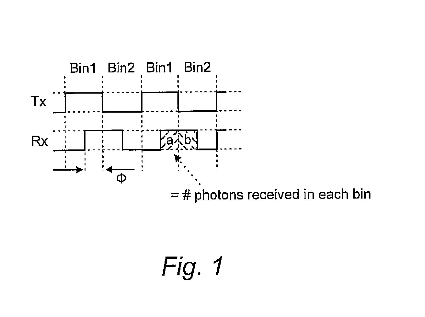
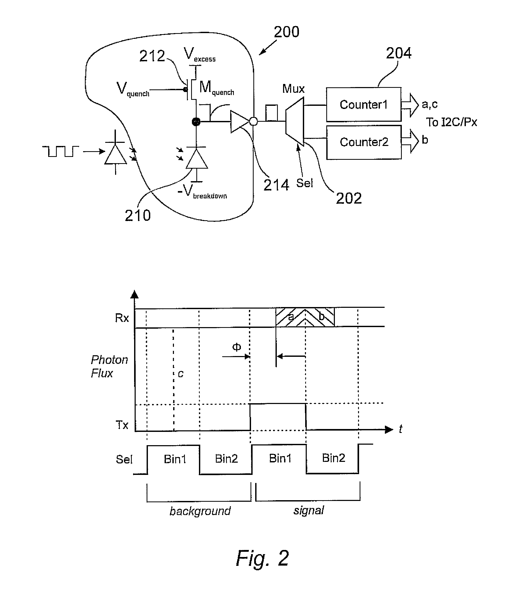
[0036]A SPAD can be used as in a ranging application through the application of a Phase Shift Extraction Method for range determination, although alternative methods exist for range determination using SPADs based on direct time of flight measurement. The term ranging in this application is intended to cover all ranging devices and methods including by not limited to ranging devices, proximity devices accelerometers etc. Ranging can occur in a number of applications, including proximity detection which is relative easy to implement and inexpensive. Laser ranging which is more complex and costly than a proximity detector, and three-dimensional imaging which is a high-end application that could be used to recognize gestures and facial expressions.

[0037]A proximity sensor is the most basic of the ranging applications. At its simplest the sensor is capable of indicating the presence or absence of a user or object by detecting the presence or absence of a reflected signal. Additional com...


PUM


Abstract

An input device for an electronic device includes a proximity detector and a light source. The light source transmits light to a sensing area, which is reflected back to the proximity detector in the presence of an object in the vicinity of the sensing area, such that the proximity detector can produce an output indicative of a distance of the object from the proximity detector to give rise to a control signal for controlling the device.

Description

FIELD OF THE INVENTION[0001]The present invention relates to an improved input device and associated method.BACKGROUND OF THE INVENTION[0002]A single photon avalanche diode (SPAR) is based on a p-n junction device biased beyond its breakdown region. The high reverse bias voltage generates a sufficient magnitude of electric field such that a single charge carrier introduced into the depletion layer of the device can cause a self-sustaining avalanche via impact ionisation. The avalanche is quenched, either actively or passively to allow the device to be “reset” to detect further photons. The initiating charge carrier can be photo-electrically generated by a single incident photon striking the high field region. It is this feature which gives rise to the name “Single Photon Avalanche Diode”. This single photon detection mode of operation is often referred to as “Geiger Mode”.[0003]U.S. Pat. No. 7,262,402 discloses an imaging device using an array of SPADs for capturing a depth and inte...

Claims


Application Information

Patent Timeline
Patent Type & Authority Applications(United States)
IPC IPC(8): G06F3/042
CPCG06F2203/04108G06F3/0428
Inventor STARK, LAURENCEHALLIDAY, WILLIAM
Owner STMICROELECTRONICS (RES & DEV) LTD
Why Eureka
Try Eureka