Active matrix device

a technology of active matrix and electrodewetting, which is applied in the direction of optics, instruments, cathode-ray tube indicators, etc., can solve the problems of not having an integrated solution with external sensor electronics, increasing cost and complexity of the overall system, and limited array elements at which impedance can be sensed

Active Publication Date: 2012-08-02
SHARP LIFE SCI EU LTD
View PDF0 Cites 18 Cited by
  • Summary
  • Abstract
  • Description
  • Claims
  • Application Information

AI Technical Summary

Benefits of technology

[0051]According to still another aspect, the multiple sets of N array elements are arranged to effect control of multiple droplets simultaneously.
[0052]According to another aspect, the multiple sets of N array elements are arra

Problems solved by technology

However a disadvantage of this method is that the number of array elements at which impedance can be sensed is limited by the number of connections that can be supplied to the device.
Furthermore this is not an integrated solution with external sensor electronics being required.
The provision of such external means (e.g. additional electr

Method used


Image

  • Active matrix device
  • Active matrix device
  • Active matrix device

Examples


first embodiment

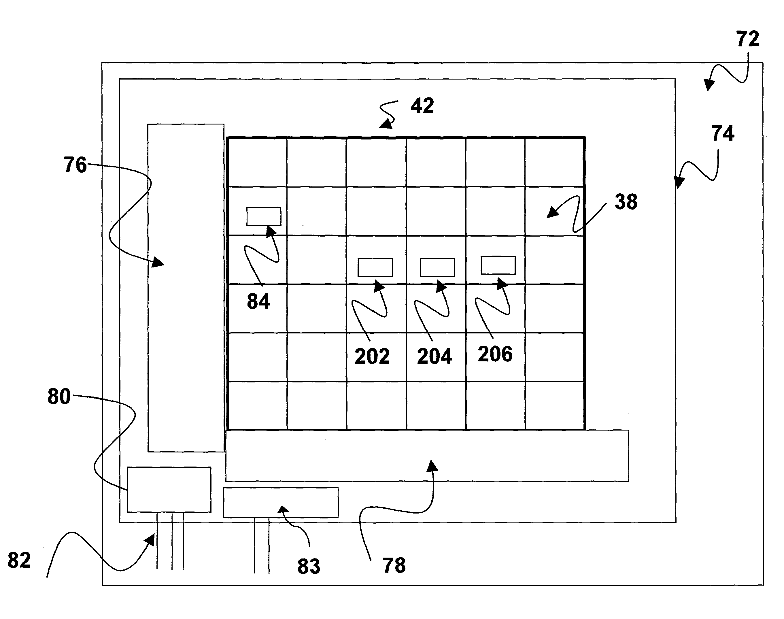
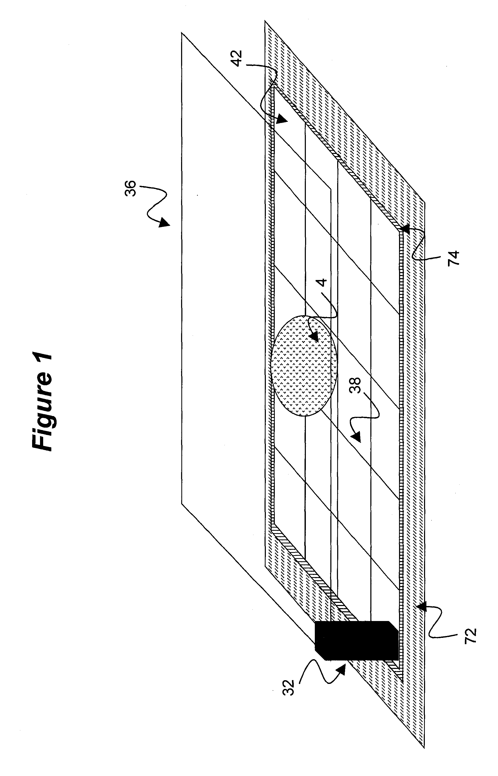
[0172]Referring initially to FIG. 1, shown is an AM-EWOD device in accordance with the present invention. The AM-EWOD device has a lower substrate 72 with thin film electronics 74 disposed upon the lower substrate 72. The thin film electronics 74 are arranged to drive array element electrodes, e.g. 38. A plurality of electrodes 38 are arranged in an electrode array 42, having M×N elements where M and N may be any number.

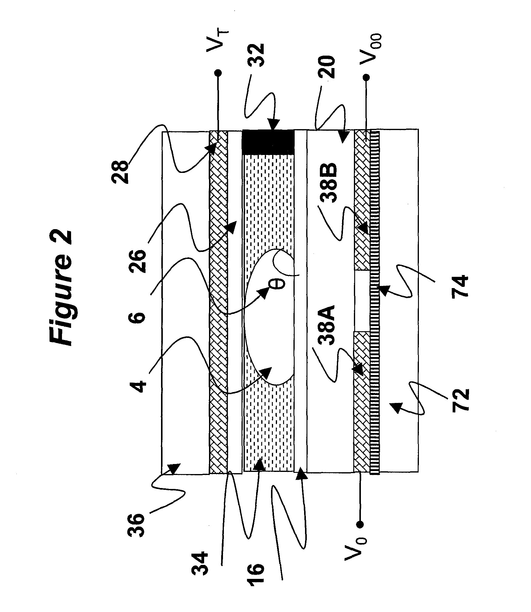
[0173]A droplet 4 is enclosed between the substrate 72 and the top substrate 36, although it will be appreciated that multiple droplets 4 can be present without departing from the scope of the invention. FIG. 2 shows array elements in cross section. The device includes the lower substrate 72 having the thin-film electronics 74 disposed thereon. An uppermost layer of the lower substrate 72 (which may be considered a part of the thin film electronics layer 74) is patterned so that a plurality of electrodes 38 (e.g., 38A and 38B) are realised. These may be termed the EW...

sixth embodiment

[0294]the invention is an AM-EWOD of conventional means and having a droplet manipulation circuit 160e as shown in FIG. 22.

[0295]The droplet manipulation circuit 160e includes the following components:

[0296]A first array element 249

[0297]A second array element 204

[0298]A third array element 206

[0299]An AND gate 222

[0300]An AND gate 224

[0301]An AND gate 252

[0302]Logical inverters 226, 228 and 230

[0303]A sensor data processing circuit 242

[0304]The sequence of array elements and logic components may be connected as follows:

[0305]The sensor output S of the first array element 249 is connected to the input of an inverter 226 and to the input SE of the sensor data processing circuit 242. The output of inverter 226 is connected to the second input of an AND gate 252. The output of AND gate 252 is connected to the write input W of the first array element 249. The output D1 of the sensor data processing circuit 242 is connected to the first input of AND gate 224. The output D2 of the sensor ...

seventh embodiment

[0319]the invention is an AM-EWOD of conventional means and having a droplet manipulation circuit 160f as shown in FIG. 25.

[0320]The droplet manipulation circuit 160f includes the following components

[0321]A first array element 202

[0322]A second array element 204

[0323]A third array element 206

[0324]AND gate 222

[0325]AND gate 224

[0326]AND gate 252

[0327]Logical inverters 226, 228 and 230

[0328]A timer control circuit 260

[0329]An OR gate 262

[0330]The sequence of array elements and logic components may be connected as follows:

[0331]The sensor output S of the first array element 202 is connected to the input of an inverter 226 and to the first input of AND gate 224, and to the timer control input T of the timer control circuit 260. The output of inverter 226 is connected to the second input of AND gate 252. The output of AND gate 252 is connected to the write input W of the first array element 202. The output of AND gate 222 is connected to the write input W of the second array element 20...


PUM


Abstract

An active matrix device is provided which includes N array elements arranged spatially in a sequence of first through Nth array elements (where N is an integer ≧2); the N array elements each including a write input for receiving a corresponding write input signal which controls operation of the array element, and a sense circuit for sensing a property of the array element and providing a sensor output based on the sensed property; and further including a manipulation circuit including logic circuitry connecting the sensor output from an nth array element in the sequence directly to the write input of an (n+1)th array element and configured to provide the write input signal to the write input of the (n+1)th array element based on the sensor output from the nth array element.

Description

TECHNICAL FIELD[0001]This invention finds application to the field of digital microfluidics and more specifically to active matrix electrowetting-on-dielectric (AM-EWOD). Electrowetting-On-Dielectric (EWOD) is a known technique for manipulating droplets of fluid on an array. AM-EWOD refers to implementation of EWOD in an active matrix array, for example by using thin film transistors (TFTs). The invention further relates to methods of driving such a device.BACKGROUND ART[0002]Electrowetting on dielectric (EWOD) is a well known technique for manipulating droplets of fluid by application of an electric field. It is thus a candidate technology for digital microfluidics for lab-on-a-chip technology. An introduction the basic principles of the technology” can be found in (“Digital microfluidics: is a true lab-on-a-chip possible?”, R. B. Fair, Microfluid Nanofluid (2007) 3:245-281).[0003]U.S. Pat. No. 6,565,727 (A. Shenderov; issued May 20, 2003) discloses a passive matrix EWOD device for...

Claims


Application Information

Patent Timeline
IPC IPC(8): G09G5/00
CPCB01L3/50273B01L3/502792B01L2200/0673B01L2200/143B01L2300/0816G09G2300/08B01L2400/0427G02F1/00G06F3/044G09G3/3648G09G3/348B01L2300/0887
Inventor HADWEN, BENJAMIN JAMESJACOBS, ADRIAN MARC SIMONHECTOR, JASON RODERICK
Owner SHARP LIFE SCI EU LTD
Why Eureka
Try Eureka