
Cooling unit, processing chamber, part in the processing chamber, and cooling method

a cooling unit and processing chamber technology, applied in the field of cooling units, can solve the problems of difficult uniform cooling of semiconductor wafers, poor temperature control responsiveness, and unnecessarily heating of semiconductor wafers or the wall of processing chambers, and achieve the effect of reducing the amount of heat medium and high efficiency

Inactive Publication Date: 2012-08-16
TOKYO ELECTRON LTD
View PDF0 Cites 9 Cited by
  • Summary
  • Abstract
  • Description
  • Claims
  • Application Information

AI Technical Summary

Benefits of technology

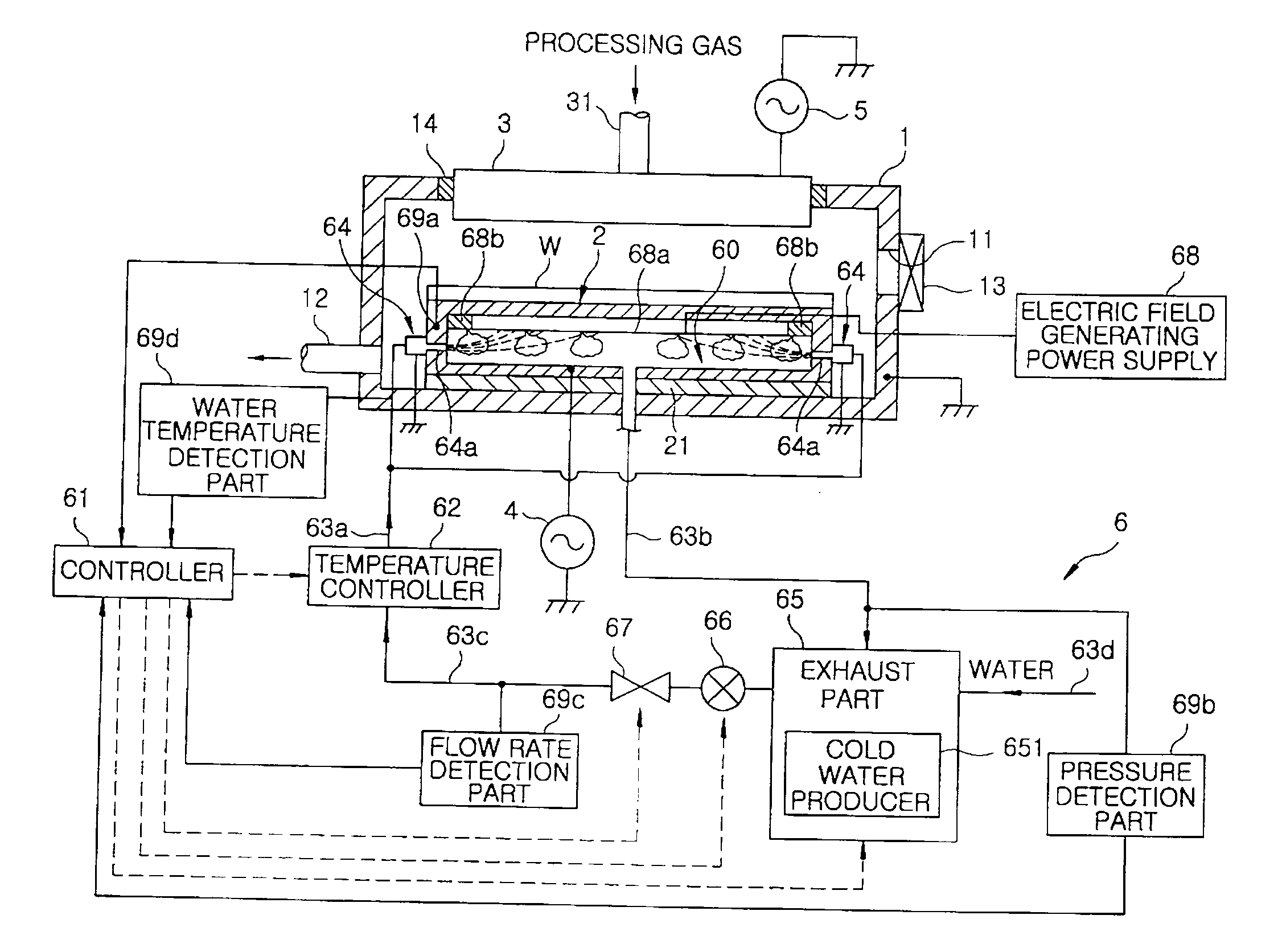
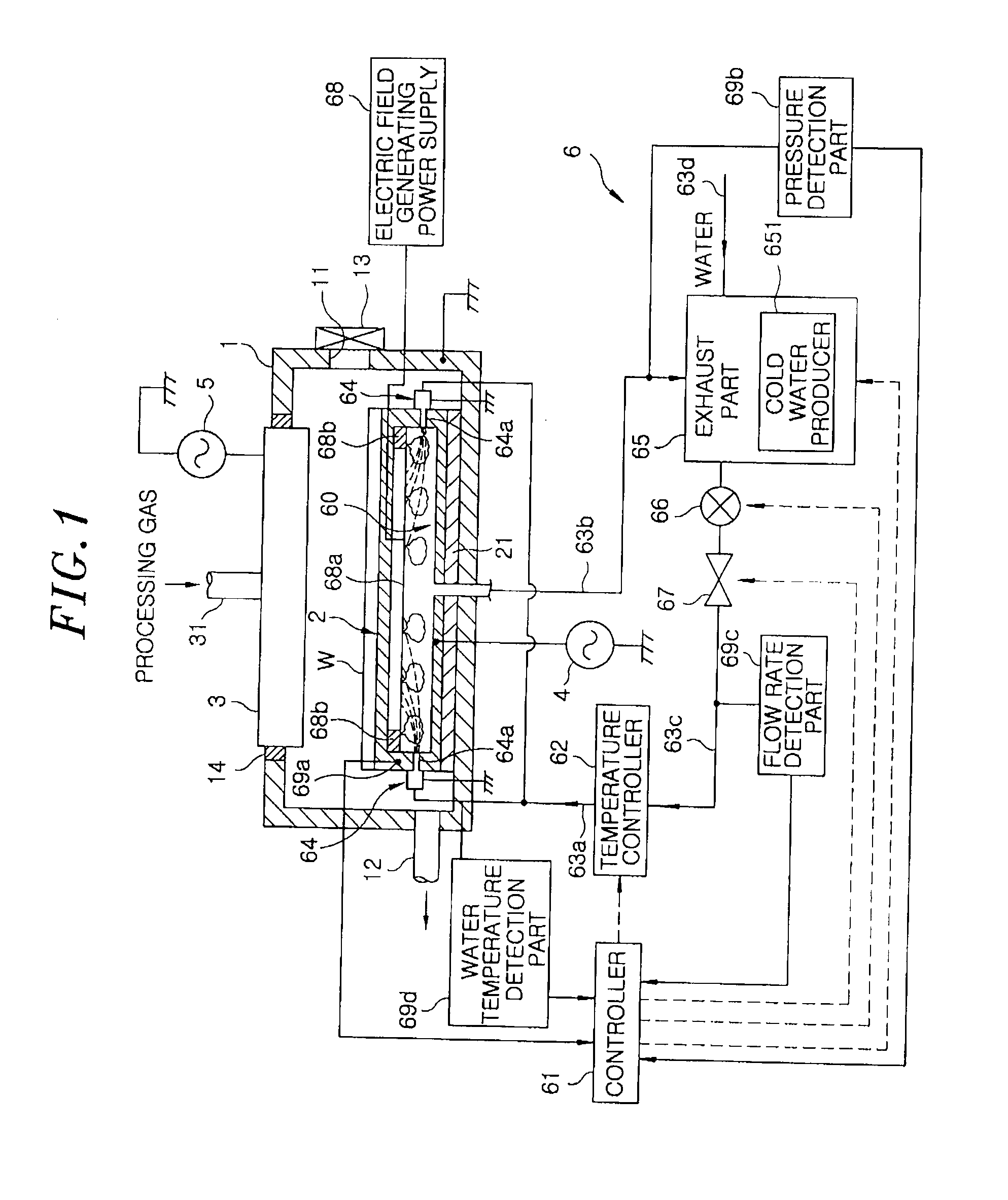
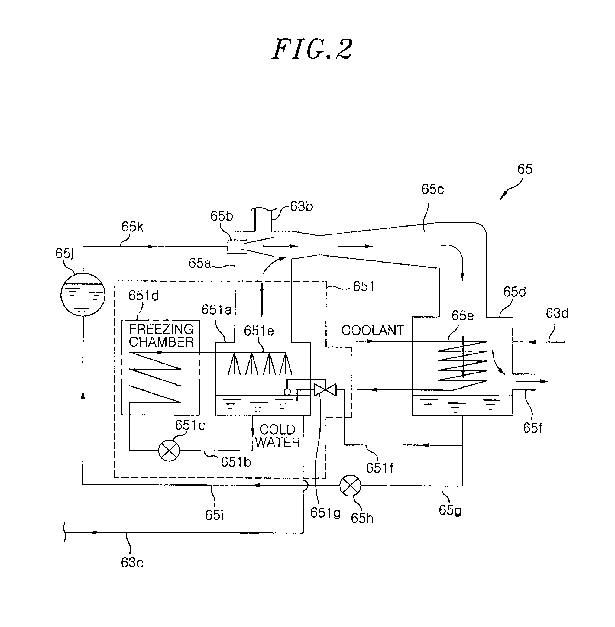
The present invention provides a cooling unit and method for cooling a target object using a decompression chamber and an electric field. The cooling unit includes a spraying part that sprays a liquid heat medium onto the inner surface of the decompression chamber, an electric field generator that attracts the heat medium to the inner surface, and an exhaust part that evacuates the decompression chamber to a pressure equal to the saturated vapor pressure of the heat medium. The cooling method involves spraying the heat medium onto the inner surface of the decompression chamber, generating an electric field to attract the heat medium, and evacuating the decompression chamber to a pressure equal to the saturated vapor pressure of the heat medium. The cooling unit and method can efficiently cool the target object and reduce the amount of heat medium required.

Problems solved by technology

However, the semiconductor wafer or the wall of a processing chamber may be unnecessarily heated by the plasma to a high temperature.
However, in cooling through the forced convection heat transfer method, since there are certain limitations on the heat transfer characteristics of the flow path, it is difficult to uniformly cool the semiconductor wafer or the like, and responsiveness to temperature control is poor.
However, since the heat transfer characteristics of the flow path is inversely related to the pressure loss, if the heat transfer characteristics of the flow path are increased, the pressure loss in the flow path becomes large, thereby increasing energy consumption of a pump for delivering the heat medium.
On the other hand, if the pressure loss is reduced in order to promote energy saving, a difference between a temperature at the inlet and that at the outlet of the heat medium becomes large, and the heat transfer characteristics of the flow path are degraded, thereby making it difficult to uniformly cool the semiconductor wafer.
However, from results of experiments, in a configuration in which the heat medium is simply sprayed to the inner surface of the decompression chamber at a low pressure, since there is no component for actively attracting the heat medium to the inner surface of the decompression chamber, the heat medium is expected to be randomly attached to the inner surface of the decompression chamber.
Accordingly, it is difficult for the liquid heat medium to be attached to the inner surface.
Therefore, it causes a new problem that it is required to supply into the decompression chamber a larger amount of heat medium than that of heat medium needed theoretically.
Further, if the amount of heat medium is increased, although the liquid heat medium may be attached to the inner surface of the decompression chamber, the heat medium supplied into the decompression chamber may not be sufficiently evacuated.
In this case, the heat medium attached to the inner surface of the decompression chamber is less likely to undergo a phase change, thereby causing a problem that it is difficult to effectively cool the mounting table.

Method used


Image

  • Cooling unit, processing chamber, part in the processing chamber, and cooling method
  • Cooling unit, processing chamber, part in the processing chamber, and cooling method
  • Cooling unit, processing chamber, part in the processing chamber, and cooling method

Examples


modification example 1

[0078]FIG. 5 schematically shows a configuration of a semiconductor manufacturing apparatus including a cooling unit 106 in accordance with Modification Example 1. The semiconductor manufacturing apparatus and the cooling unit 106 in accordance with Modification Example 1 have the same configurations as those of the above-described embodiment, and further include a voltage application part 164b to apply a voltage to the spraying part 64. The voltage application part 164b is a DC power supply for electrically charging the water sprayed from the spraying part 64. In a case where the electric field directed from the inside of the decompression chamber 60 toward the top surface portion of the decompression chamber 60 is generated by the electric field generating power supply 68, a positive potential is applied to the spraying part 64. In a case where the electric field directed from the top surface portion of the decompression chamber 60 toward the inside of the decompression chamber 60...

modification example 2

[0080]FIG. 6 schematically shows a configuration of a semiconductor manufacturing apparatus including a cooling unit 206 in accordance with Modification Example 2. The semiconductor manufacturing apparatus and the cooling unit 206 in accordance with Modification Example 2 have the same configurations as those of the above-described embodiment, and are different from those of the above embodiment in that a decompression chamber 260 and a spraying part 264 are further provided in the wall of a processing chamber (target object to be cooled) 201, so that a desired location of the inner wall of the processing chamber 201 is cooled. The desired location of the inner wall of the processing chamber 201 may be a part of the inner wall, or the whole inner wall. The difference will be mainly described below.

[0081]The processing chamber 201 of the semiconductor manufacturing apparatus in accordance with Modification Example 2 has the decompression chamber 260 formed in the wall thereof to cool...

modification example 3

[0087]FIG. 7 schematically shows a configuration of a semiconductor manufacturing apparatus including a cooling unit 306 in accordance with Modification Example 3. The cooling unit 306 in accordance with Modification Example 3 has a first and a second decompression chamber 360 and 370 for cooling the mounting table 2 as a target object to be cooled and a processing chamber (target object to be cooled) 301, respectively, wherein the first decompression chamber 360 is provided at an external of the mounting table 2 and the second decompression chamber 370 is provided at an external of the processing chamber 301.

[0088]The first decompression chamber 360 is formed in a hollow cylindrical shape, and fixed onto an approximately central bottom portion of the processing chamber 301. The mounting table 2 is fixed on the top of the first decompression chamber 360 through the disc-shaped insulator 21. The first decompression chamber 360 has the same configuration as the decompression chamber 6...


PUM


Abstract

A cooling unit for cooling a target object to a target temperature includes a decompression chamber thermally connected to the target object; a spraying part which sprays a liquid heat medium having a temperature equal to or lower than the target temperature to an inner surface of the decompression chamber; and an electric field generator which generates an electric field such that the heat medium sprayed from the spraying part is attached to the inner surface of the decompression chamber. The cooling unit further includes an exhaust part which evacuates the decompression chamber such that a pressure in the decompression chamber is equal to or lower than a saturated vapor pressure of the heat medium at the target temperature.

Description

FIELD OF THE INVENTION[0001]The present invention relates to a cooling unit and a cooling method for controlling a temperature of a target object to be cooled to and be maintained at a target temperature, and a processing chamber and a part in the processing chamber forming the cooling unit.BACKGROUND OF THE INVENTION[0002]In a semiconductor manufacturing apparatus, a plasma is frequently used to perform a processing such as an etching on a semiconductor wafer as a target object to be processed. However, the semiconductor wafer or the wall of a processing chamber may be unnecessarily heated by the plasma to a high temperature. Further, although there is a semiconductor manufacturing apparatus in which the semiconductor wafer needs to be processed at a high temperature, cooling is required after the processing for transferring and for another processing even in such apparatus. Accordingly, the semiconductor manufacturing apparatus includes a cooling unit for cooling the semiconductor...

Claims


Application Information

Patent Timeline
Patent Type & Authority Applications(United States)
IPC IPC(8): F25B21/00
CPCH01L21/67017H01L21/67253H01L21/67109H01L21/02H01L21/3065
Inventor MATSUZAKI, KAZUYOSHIOIKAWA, JUNJINAGASEKI, SUMIE
Owner TOKYO ELECTRON LTD
Learn More