Ground protection circuit and switch driving device using the same

a technology of ground protection circuit and driving device, which is applied in the direction of circuit arrangement, emergency protection circuit arrangement, electrical equipment, etc., can solve the problems of switching sw or load damage, driving current i is turned into an overcurrent state, etc., and achieve the effect of increasing cost and reducing output efficiency

Active Publication Date: 2012-08-23
ROHM CO LTD
View PDF5 Cites 7 Cited by
  • Summary
  • Abstract
  • Description
  • Claims
  • Application Information

AI Technical Summary

Benefits of technology

[0016]According to the present invention, a ground protection circuit which can perform proper ground protection without increasing the cost or reducing the output efficiency and a switch driving device using the same are provided.

Problems solved by technology

In the switch driving device, when a connection end of the load is grounded (the grounding end or a low potential end equivalent to the grounding end is short-circuited), the driving current I is turned into an overcurrent state and the switch SW or load can be damaged.

Method used


Image

  • Ground protection circuit and switch driving device using the same
  • Ground protection circuit and switch driving device using the same
  • Ground protection circuit and switch driving device using the same

Examples


first embodiment

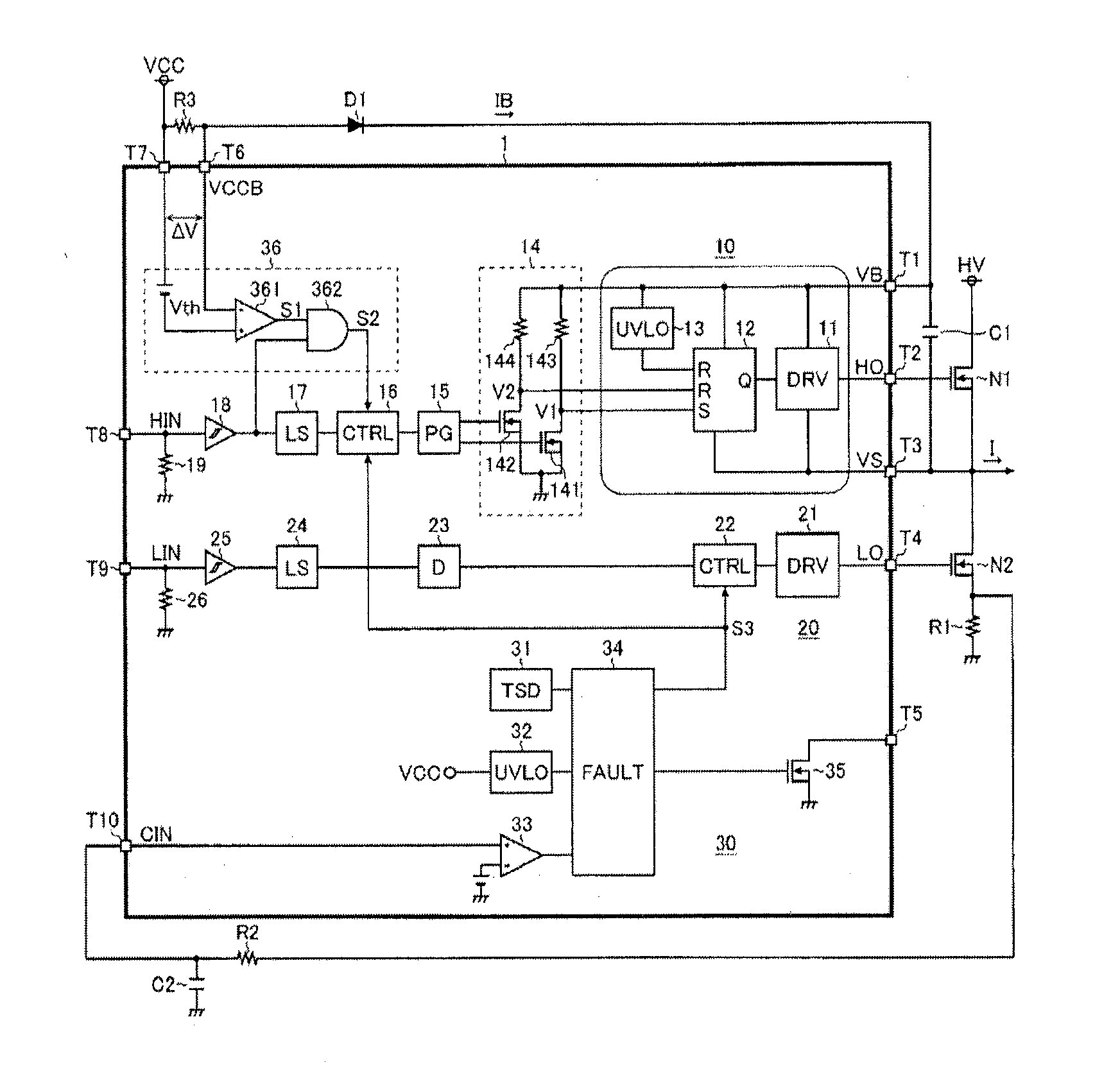
[0026]FIG. 1 is a block diagram showing a switch driving device according to a first embodiment of the present invention. A switch driving device 1 of the first embodiment is a single-chip semiconductor integrated circuit device including an upper switch driving portion 10, a lower switch driving portion 20 and a fault protection portion 30. The switch driving device 1 controls a driving current I of a load (not shown) by controlling the on / off of N channel metal oxide semiconductor (MOS) field effect transistors N1 and N2 connected to the outside of the switch driving device 1.

[0027]The switch driving device 1 includes external terminals T1 to T10 so as to determine the electrical connection to the outside of the device. In addition to being connected to the transistors N1 and N2 used as on / off control objects, the outside of the switch driving device 1 is further connected to resistors R1 to R3, capacitors C1 and C2, and a diode D1.

[0028]At the outside of the switch driving device...

second embodiment

[0070]FIG. 4 is a block diagram showing a switch driving device according to a second embodiment of the present invention. The switch driving device 1 of the second embodiment is of the substantially same configuration with that of the first embodiment, and is characterized by that the resistor R3 is built in. Through the configuration, the number of external discrete parts can be reduced, thereby facilitating the cost reduction or miniature of the set.

[0071]FIG. 5 is a circuit diagram showing a configuration example of a resistor R3. As shown in the configuration example, the resistor R3 can be implemented by using the on-resistance of a P channel MOS field effect transistor. Through the configuration, the resistance value of the resistor R3 built in the switch driving device 1 can be sufficiently high, and therefore, like the situation that the resistor R3 is built out, the resistor R3 can not only be used as the sensing resistor, but also can be concurrently used as the limiting ...


PUM


Abstract

A ground protection circuit (36) includes: a sensing resistor (R3), disposed on a path which a charging current (IB) of a bootstrap circuit (D1, C1) flows through; a comparator (361), for comparing a voltage (ΔV) between two ends of the sensing resistor (R3) and a specific threshold voltage (Vth) to generate a ground protection signal (S1); and a logic gate (362), for enabling the ground protection signal (S1) to be invalid in a normal charging operation of the bootstrap circuit.

Description

BACKGROUND OF THE INVENTION[0001]1. Field of the Invention[0002]The present invention relates to a ground protection circuit and a switch driving device using the same.[0003]2. Description of the Related Art[0004]FIG. 9 is a diagram showing a conventional switch driving device having a ground protection circuit. The conventional switch driving device is a semiconductor integrated circuit device which controls a driving current I of a load by performing on / off control on a switch SW. In the switch driving device, when a connection end of the load is grounded (the grounding end or a low potential end equivalent to the grounding end is short-circuited), the driving current I is turned into an overcurrent state and the switch SW or load can be damaged. Therefore, the conventional switch driving device has a ground protection circuit, so as to monitor a voltage ΔV between two ends of a sensing resistor Rs mounted on a current path of the driving current I, and to compulsorily switch off ...

Claims


Application Information

Patent Timeline
Patent Type & Authority Applications(United States)
IPC IPC(8): H02H3/02
CPCH02H3/087H02H7/222H02H7/20
Inventor ANDO, MOTOHIRO
Owner ROHM CO LTD
Why Eureka
Try Eureka