Non-volatile memory structure and method for manufacturing the same

Inactive Publication Date: 2012-09-06
EMEMORY TECH INC
View PDF4 Cites 13 Cited by
  • Summary
  • Abstract
  • Description
  • Claims
  • Application Information

AI Technical Summary

Benefits of technology

[0011]In the non-volatile memory structure, the fabrication process is compatible with a CMOS manufacturing process. In addition, the charge-trapping layer is disposed between the two gates f

Problems solved by technology

However, the fabrication of

Method used


Image

  • Non-volatile memory structure and method for manufacturing the same
  • Non-volatile memory structure and method for manufacturing the same
  • Non-volatile memory structure and method for manufacturing the same

Examples


Example

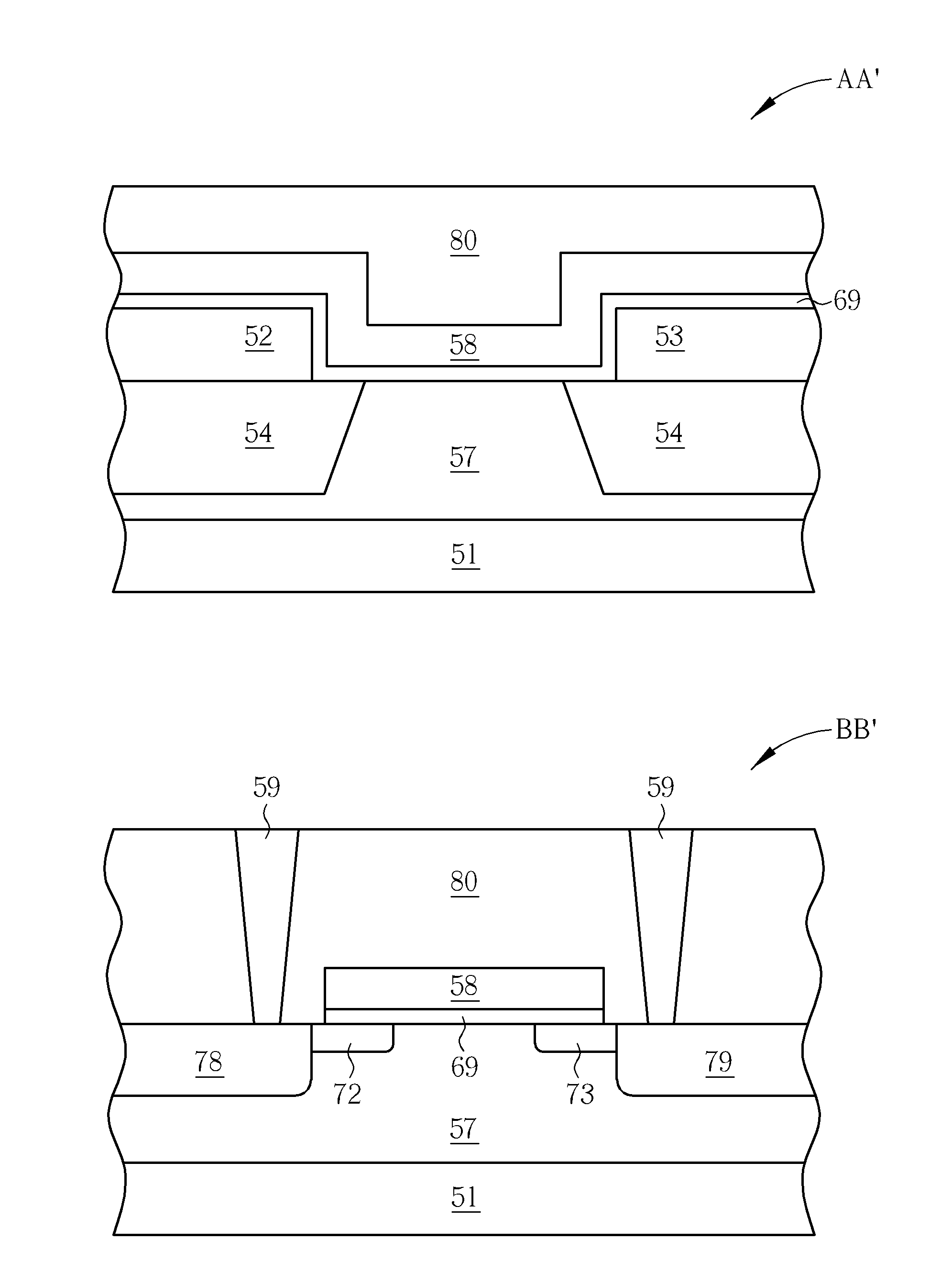
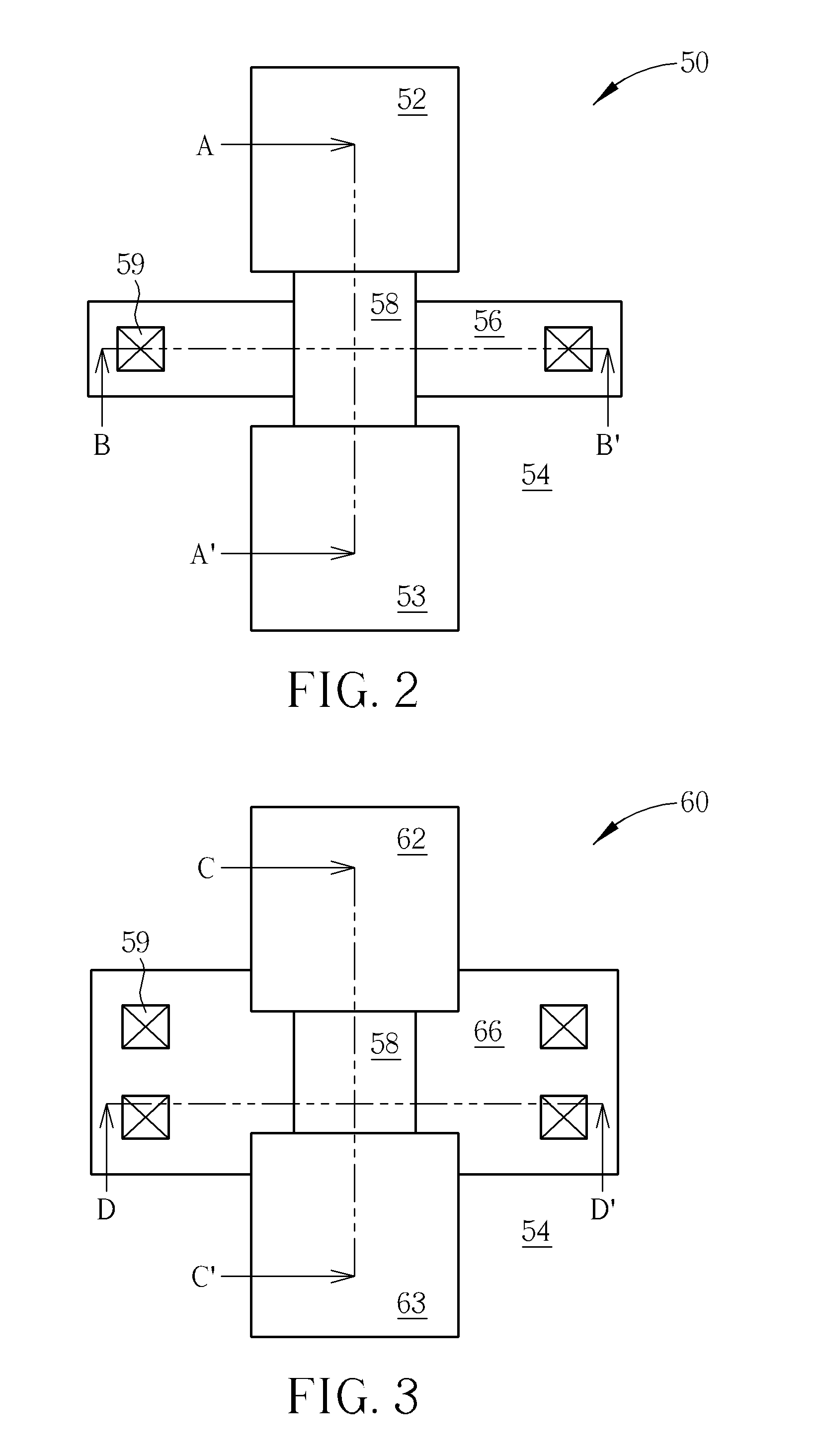
[0018]Referring to FIG. 2, in a non-volatile memory structure 50 according to the present invention, a first gate 52 and a second gate 53 are each entirely disposed on an isolation structure 54 and opposite each other. The isolation structure 54 surrounds an active area 56, both disposed within a substrate (not shown) . The active area 56 has a portion (a middle region) between the first gate 52 and the second gate 53. A dielectric layer (not shown) is disposed on a sidewall of each of the first gate 52 and the second gate 53 and on the substrate between the first gate 52 and the second gate 53. The dielectric layer may be for example a liner dielectric, such as a liner oxide. A charge-trapping layer 58 is disposed on the dielectric layer, such that the charge-trapping layer 58 is also between the first gate 52 and the second gate 53. The charge-trapping layer 58 and the dielectric layer together serve for a storage node function. A pair of source / drain regions (not shown) are forme...


PUM


Abstract

A non-volatile memory structure is disclosed. LDD regions may be optionally formed through an ion implantation using a mask for protection of a gate channel region of an active area. Two gates are apart from each other and disposed on an isolation structure on two sides of a middle region of the active area, respectively. The two gates may be each entirely disposed on the isolation structure or partially to overlap a side portion of the middle region of the active area. A charge-trapping layer and a dielectric layer are formed between the two gates and on the active area to serve for a storage node function. They may be further formed onto all sidewalls of the two gates to serve as spacers. Source/drain regions are formed through ion implantation using a mask for protection of the gates and the charge-trapping layer.

Description

CROSS REFERENCE TO RELATED APPLICATIONS[0001]This application claims the benefit of U.S. Provisional Application No. 61 / 449,074, filed on Mar. 3, 2011 and entitled “method of manufacturing non-volatile memory device,” the contents of which are incorporated herein by reference.BACKGROUND OF THE INVENTION[0002]1. Field of the Invention[0003]The present invention relates to a semiconductor structure and process, and particularly to a memory structure and method for manufacturing the same.[0004]2. Description of the Prior Art[0005]Non-volatile memory (NVM) is a type of memory that retains information even when no power is supplied to memory blocks thereof. Some examples include magnetic devices, optical discs, flash memory, and other semiconductor-based memory technologies. As semiconductor memory techniques have matured, one advantage that has come out is the ability to integrate substantial amounts of memory cells in integrated circuits (ICs). However, it is desirable that the memory ...

Claims


Application Information

Patent Timeline
IPC IPC(8): H01L21/336H01L29/792
CPCH01L21/28282H01L29/792H01L29/66833H01L29/42344H01L29/40117
Inventor LU, HAU-YANCHEN, HSIN-MINGYANG, CHING-SUNG
Owner EMEMORY TECH INC
Why Eureka
Try Eureka