Multilayer substrate and method for producing the same, diamond film and method for producing the same

a diamond film and multi-layer substrate technology, applied in the direction of crystal growth process, polycrystalline material growth, transportation and packaging, etc., can solve the problems of high production cost, long production time, complex step, etc., and achieve low cost, large area, and high quality.

Inactive Publication Date: 2012-09-06
SHIN ETSU CHEM CO LTD
View PDF1 Cites 0 Cited by
  • Summary
  • Abstract
  • Description
  • Claims
  • Application Information

AI Technical Summary

Benefits of technology

[0014]However, this method needs to perform the heteroepitaxial growth twice. Therefore, its production time is long, its step is complex and its production cost is high. Further, since the single crystal MgO substrate has a lot of defects, defects easily occur in the Ir film and the diamond film formed on the substrate surface. Moreover, since the difference of a linear expansion coefficient between the single crystal MgO substrate and the diamond film is large, the single crystal MgO substrate or the diamond film is broken by a stress difference.
[0015]The present invention was accomplished in order to solve the aforementioned problems, and its object is to provide a multilayer substrate having a high quality single crystal diamond film with a large area and with a high crystallinity as a continuous film in which the diamond and the single crystal substrate are not broken and a method for producing the multilayer substrate at low cost.

Problems solved by technology

However, this method needs to perform the heteroepitaxial growth twice.
Therefore, its production time is long, its step is complex and its production cost is high.
Further, since the single crystal MgO substrate has a lot of defects, defects easily occur in the Ir film and the diamond film formed on the substrate surface.

Method used


Image

  • Multilayer substrate and method for producing the same, diamond film and method for producing the same
  • Multilayer substrate and method for producing the same, diamond film and method for producing the same
  • Multilayer substrate and method for producing the same, diamond film and method for producing the same

Examples


Embodiment Construction

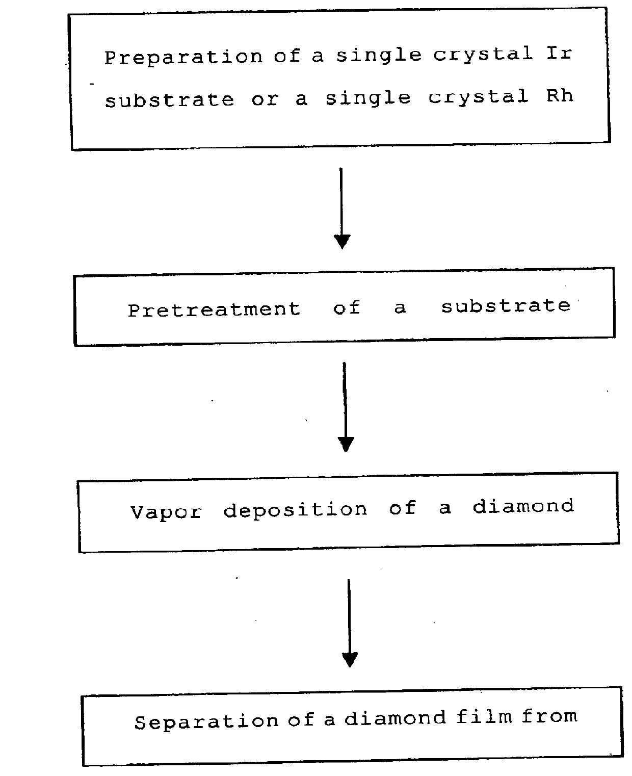
[0041]Hereinafter, embodiments of the present invention will be explained. However, the present invention is not limited by these explanations.

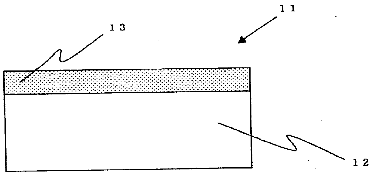
[0042]As mentioned above, the conventional multilayer substrate had a problem that a MgO substrate or a diamond is easily broken particularly due to stress caused by the difference of a linear expansion coefficient between the MgO substrate and the diamond film, and particularly a single crystal diamond film with a large area cannot be obtained as a continuous film.

[0043]Accordingly, the present inventor diligently studied for solving such a problem.

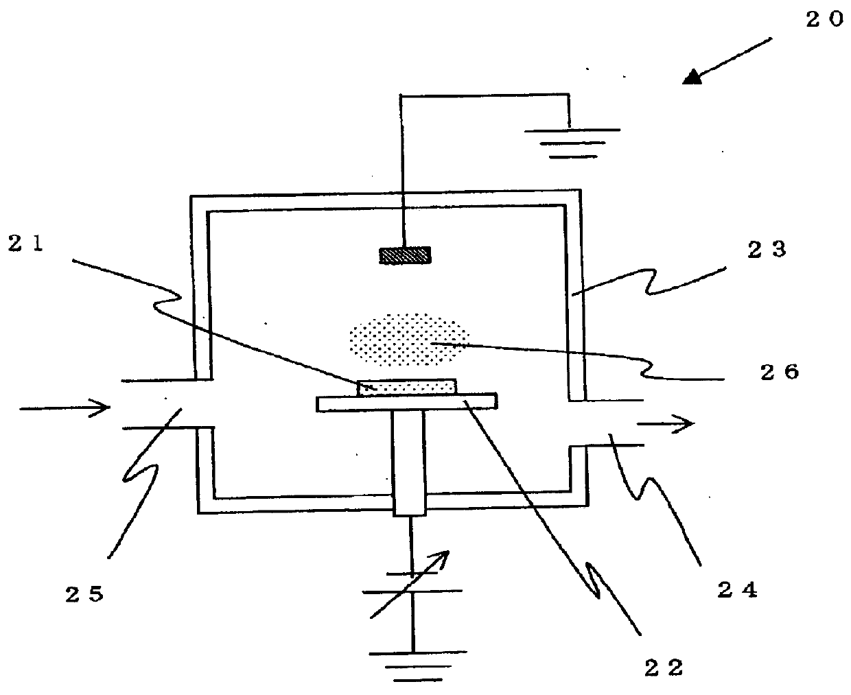
[0044]As a result, the present inventor found that if a single crystal in which the difference of a linear expansion coefficient from that of a diamond is as small as possible is used as a single crystal to be a substrate, and if a diamond film is vapor-deposited on the single crystal, a high quality diamond film can be obtained on the substrate even if it has a large area. Thereby, the present in...


PUM

PropertyMeasurementUnit
dielectric breakdown electric fieldaaaaaaaaaa
diameteraaaaaaaaaa
pressureaaaaaaaaaa

Abstract

The present invention is a multilayer substrate comprising, at least, a single crystal substrate, a diamond film vapor-deposited on the single crystal substrate, wherein the single crystal substrate is a single crystal Ir or a single crystal Rh and a method for producing a multilayer substrate comprising, at least, a step of vapor-depositing a diamond film on a single crystal substrate, wherein a single crystal Ir or a single crystal Rh is used as the single crystal substrate. As a result, there is provided a multilayer substrate having a high quality single crystal diamond film with a large area and with a high crystallinity as a continuous film in which the diamond and the single crystal substrate are not broken and a method for producing the multilayer substrate at low cost.

Description

PRIORITY INFORMATION[0001]This is a Division of application Ser. No. 12 / 654,797 filed Jan. 4, 2010, which claims the benefit of Japanese Application No. 2009-003088 filed Jan. 9, 2009. The disclosure of each of the prior applications is hereby incorporated by reference herein in its entirety.BACKGROUND OF THE INVENTION[0002]1. Field of the Invention[0003]The present invention relates to a multilayer substrate used for production of devices and the like, and particularly a multilayer substrate having a diamond film.[0004]2. Description of the Related Art[0005]Diamond has a wide band gap of 5.47 eV and a very high dielectric breakdown electric field intensity of 10 MV / cm. Furthermore, it has the highest thermal conductivity in materials. Therefore, if this is used for an electronic device, the device is advantageous as a high output electronic device.[0006]Furthermore, diamond has a high drift mobility and is the most advantageous as a high speed electronic device in semiconductors in...

Claims


Application Information

Patent Timeline
Patent Type & Authority Applications(United States)
IPC IPC(8): B32B15/04C01B31/00
CPCC30B25/105C30B29/04C30B25/18Y10T428/31678
Inventor NOGUCHI, HITOSHI
Owner SHIN ETSU CHEM CO LTD
Why Eureka
Try Eureka