

Field-effect transistor, semiconductor wafer, method for producing field-effect transistor and method for producing semiconductor wafer
a field-effect transistor and semiconductor wafer technology, applied in the direction of semiconductor devices, electrical appliances, basic electric elements, etc., can solve the problem of carrier mobility falling
- Summary
- Abstract
- Description
- Claims
- Application Information
AI Technical Summary
Benefits of technology
Problems solved by technology
Method used
Image

Examples
first working example
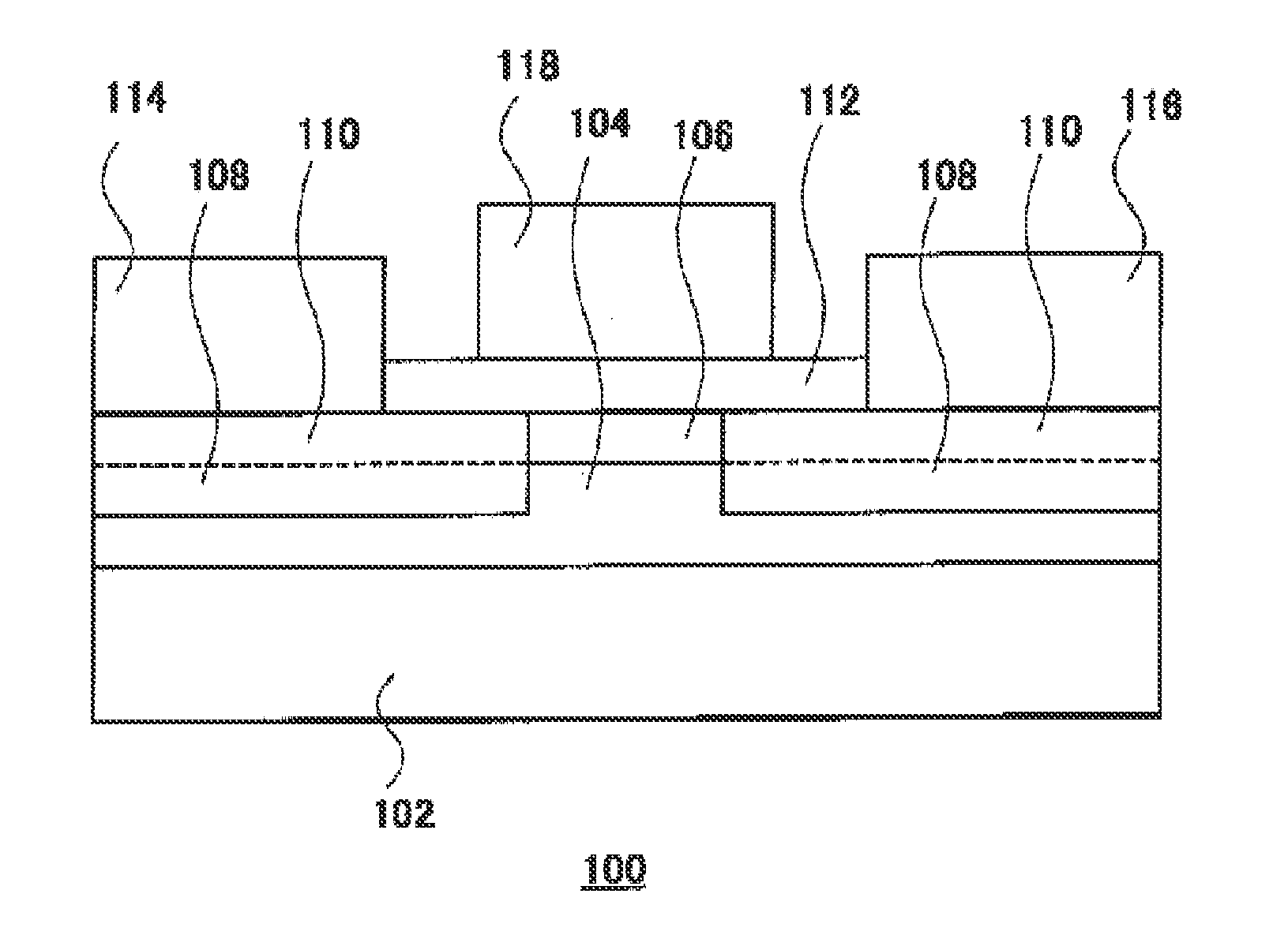
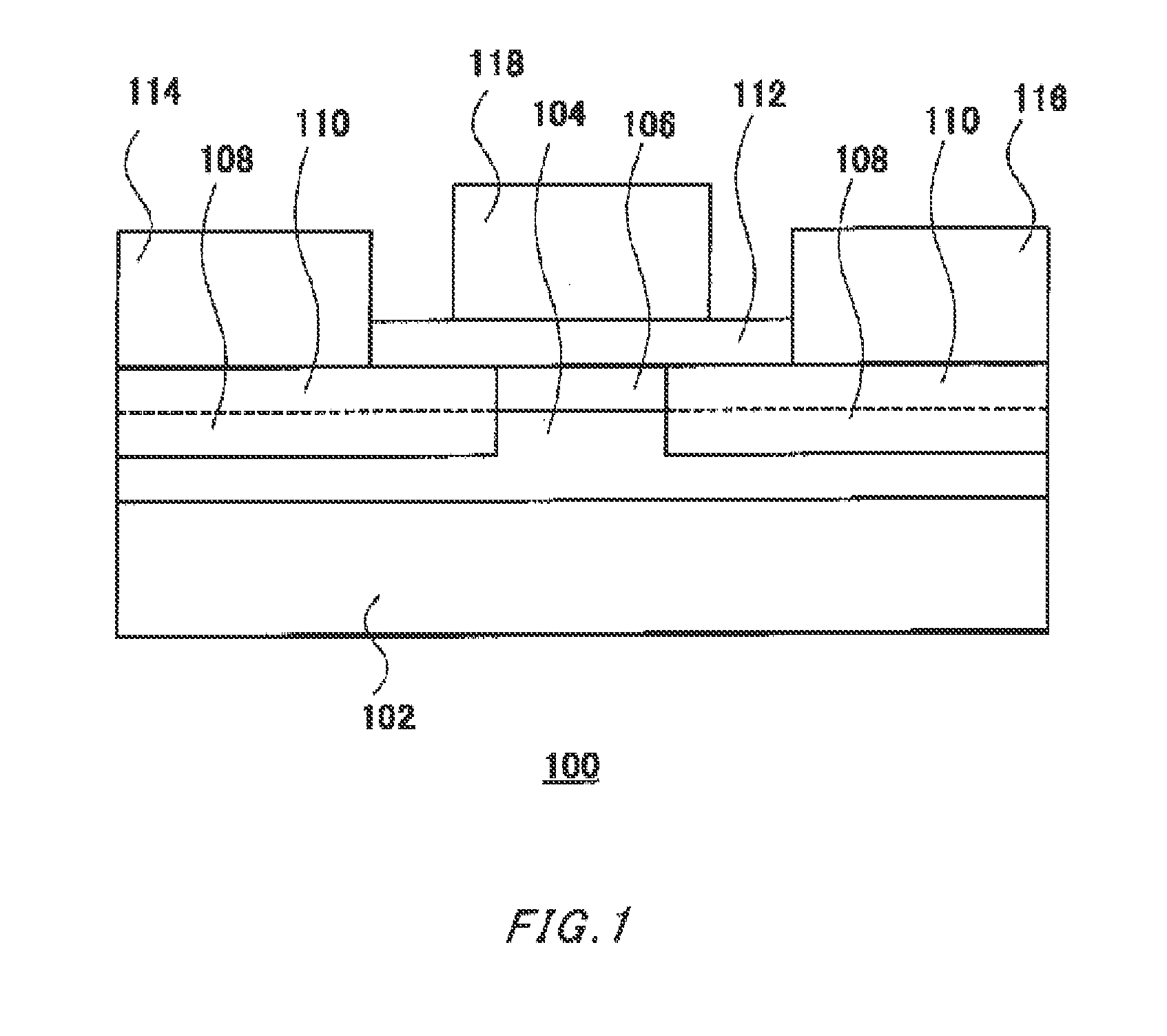
[0096]FIG. 8 is a cross-sectional view illustrating a field-effect transistor 500 relating to a working example of the present invention. FIGS. 9 to 14 show the cross-sections observed during the producing process of the field-effect transistor 500.
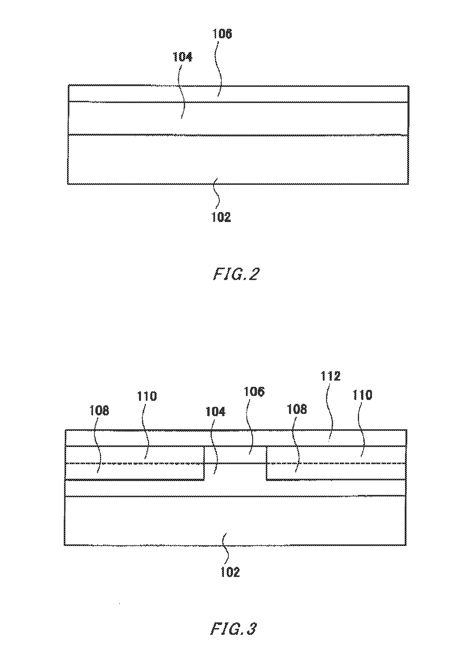
[0097]As shown in FIG. 9, a P-type InP wafer 502 was provided. On the (001) plane of the InP wafer 502, a P-type InGaAs layer 504 and an I-type InP layer 506 were epitaxially grown. Referring to the InGaAs layer 504, the composition was In0.53Ga0.47As and the concentration of the P-type impurities was 3×1016 cm−3. On the InP layer 506, a sacrificial protective layer 508 was formed to prevent Group VB atoms from leaking. As the sacrificial protective layer 508, Al2O3 was formed to a thickness of 6 nm.
[0098]As shown in FIG. 10, a mask 510 was formed and Si atoms were introduced by ion implantation. The ion implantation was performed with an implantation energy of 30 keV and an implantation amount of 2×1014 cm−2.
[0099]As shown in FIG. 11, th...
second working example
[0106]FIG. 16 is a cross-sectional view illustrating a field-effect transistor 600 relating to another working example of the present invention. The field-effect transistor 600 does not have the N-type layer 514 of the InP layer 506, which constitutes part of the field-effect transistor 500.
[0107]FIGS. 17 to 24 illustrate cross-sections observed during the producing process of the field-effect transistor 600. As in the first working example, a P-type InGaAs layer 504 and an I-type InP layer 506 were epitaxially grown on a P-type InP wafer 502, and a sacrificial protective layer 505 was formed on the InP layer 506 as shown in FIG. 17. The respective layers have the same compositions, impurity concentrations and thicknesses as in the first working example. On the sacrificial protective layer 508, a mask 510 was formed. The mask 510 was a photoresist film and formed to cover a region in which the gate electrode 524 was to be formed.
[0108]As shown in FIG. 18, the mask 510 was used as a ...
PUM
 Abstract
Description
Claims
Application Information