Eureka AIR delivers breakthrough ideas for toughest innovation challenges, trusted by R&D personnel around the world.

Silicon heterojunction solar cell and back field structure thereof, and preparation method of back field structure

A solar cell, silicon heterojunction technology, applied in circuits, photovoltaic power generation, electrical components, etc., can solve problems such as reducing the hole collection efficiency of solar cells, and achieve the effect of improving conversion efficiency

Pending Publication Date: 2020-07-03
德运创鑫(北京)科技有限公司
View PDF0 Cites 0 Cited by
  • Summary
  • Abstract
  • Description
  • Claims
  • Application Information

AI Technical Summary

Problems solved by technology

[0004] The back field of the existing p-type silicon heterojunction solar cells has a high Schottky barrier to holes at the interface between the TCO layer and the p-type silicon doped layer, so the holes in the p-type silicon substrate need to cross the Schottky barrier. The base barrier can be collected by the solar cell, which reduces the collection efficiency of the solar cell for holes

Method used


Image

  • Silicon heterojunction solar cell and back field structure thereof, and preparation method of back field structure
  • Silicon heterojunction solar cell and back field structure thereof, and preparation method of back field structure
  • Silicon heterojunction solar cell and back field structure thereof, and preparation method of back field structure

Examples


Embodiment Construction

[0057] In order to make the purpose, technical solution and advantages of the application clearer, the embodiments of the application will be described in detail below in conjunction with the accompanying drawings. It should be noted that, in the case of no conflict, the embodiments in the present application and the features in the embodiments can be combined arbitrarily with each other.

[0058] In the present application, "more layers" means two or more layers, and "more kinds" means two or more layers, unless otherwise specifically defined.

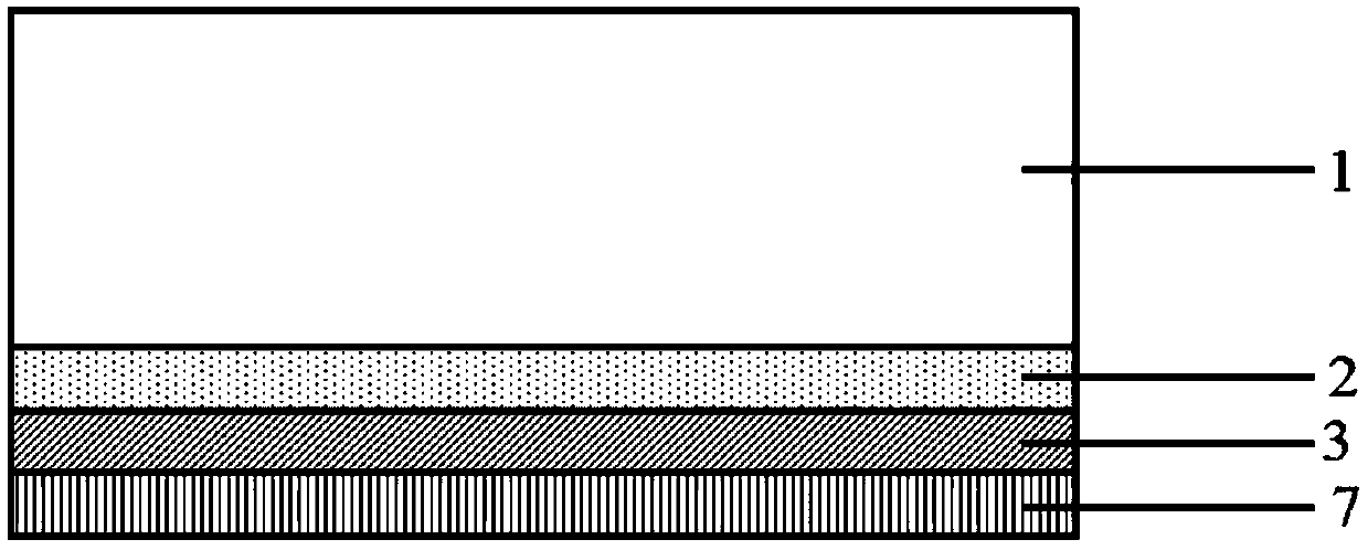
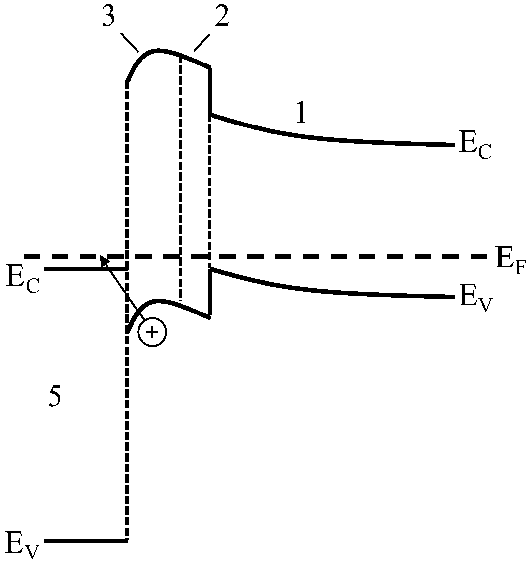
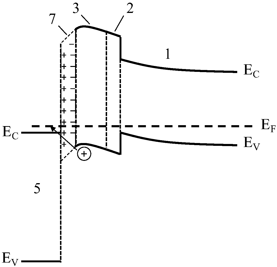
[0059] The embodiment of the present application provides a back field structure of a silicon heterojunction solar cell, such as figure 1 As shown, the back field structure includes:

[0060] A p-type silicon substrate 1, the p-type silicon substrate 1 has a back field surface;

[0061] a first intrinsic passivation layer 2 formed on the back field surface;

[0062] a p-type silicon doped layer 3 formed on the first intrinsic passi...


PUM

PropertyMeasurementUnit
thicknessaaaaaaaaaa
thicknessaaaaaaaaaa

Abstract

The invention discloses a silicon heterojunction solar cell back field structure, which comprises: a p-type silicon substrate provided with a back field surface; a first intrinsic passivation layer formed on the back field surface; a p-type silicon doped layer formed on the first intrinsic passivation layer; and an adsorption atom layer formed on the p-type silicon doped layer, wherein the adsorption atom layer comprises adsorption atoms which are deposited on the surface of the p-type silicon doped layer and form a positive dipole moment potential field with the silicon atoms on the surface of the p-type silicon doped layer. The invention also discloses a preparation method of the silicon heterojunction solar cell back field structure and a silicon heterojunction solar cell. The Schottkybarrier of the p-type silicon doped layer and the TCO interface of the back field structure to the hole of the p-type silicon substrate is low in height, and the filling factor and the conversion efficiency of the silicon heterojunction solar cell are high.

Description

technical field [0001] The present application relates to but not limited to the field of photovoltaic technology, and particularly relates to but not limited to a silicon heterojunction solar cell, its back field structure and a method for preparing the back field structure. Background technique [0002] Silicon heterojunction (SHJ) solar cells have been widely used in photovoltaic academia and industry in recent years because of their outstanding advantages such as high open circuit voltage, high conversion efficiency, low temperature coefficient, simple process flow, and no light-induced attenuation. Attention has become a popular development direction of high-efficiency solar cell technology. [0003] At present, the basic structure of a p-type silicon heterojunction solar cell is: an intrinsic passivation layer is deposited on both sides of a p-type silicon substrate, a p-type silicon doped layer is deposited on the intrinsic passivation layer on one side, and a p-type ...

Claims


Application Information

Patent Timeline
Patent Type & Authority Applications(China)
IPC IPC(8): H01L31/0747H01L31/0352H01L31/20
CPCH01L31/035272H01L31/0747H01L31/202H01L31/204Y02E10/50Y02P70/50
Inventor 龙巍
Owner 德运创鑫(北京)科技有限公司
Why Eureka
Eureka Blog
Learn More