
Dielectric Waveguide Filter

a filter and waveguide technology, applied in waveguides, resonators, electrical equipment, etc., can solve the problem of increasing the loss of insertion in the passband of the filter, and achieve the effect of increasing the distan

Inactive Publication Date: 2012-09-13
MURATA MFG CO LTD
View PDF2 Cites 22 Cited by
  • Summary
  • Abstract
  • Description
  • Claims
  • Application Information

AI Technical Summary

Benefits of technology

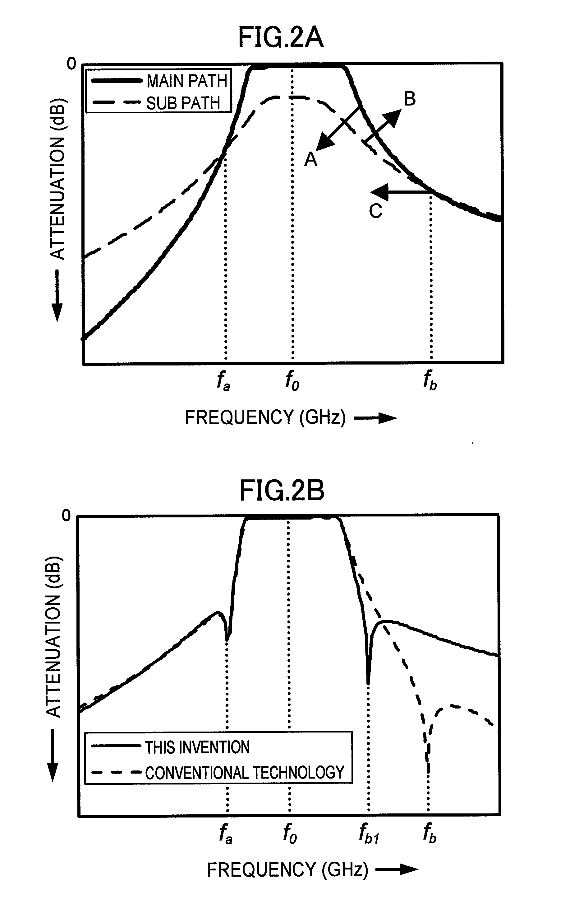
[0023]In one aspect of the present invention, a capacitive coupling path is used in the part of the main coupling path, so that it becomes possible to provide a dielectric waveguide filter in which a high band-side attenuation pole comes close to a center frequency, and an attenuation characteristic become steep on both of high band and low band sides.
[0024]In another aspect of the present invention, a dielectric plate having a dielectric constant greater than that of the dielectric waveguide resonator is inserted in the capacitive coupling path, so that it becomes possible to increase a distance between opposed sides of the capacitive window in a short-side direction thereof to provide a dielectric waveguide filter in which electric discharge is less likely to occur in the capacitive window even when a large amount of electric power is input into the dielectric waveguide filter.

Problems solved by technology

Thus, if the number of dielectric waveguide resonators in a dielectric waveguide filter is increased, an insertion loss in a passband of the filter will be increased.

Method used


Image

  • Dielectric Waveguide Filter
  • Dielectric Waveguide Filter
  • Dielectric Waveguide Filter

Examples


first embodiment

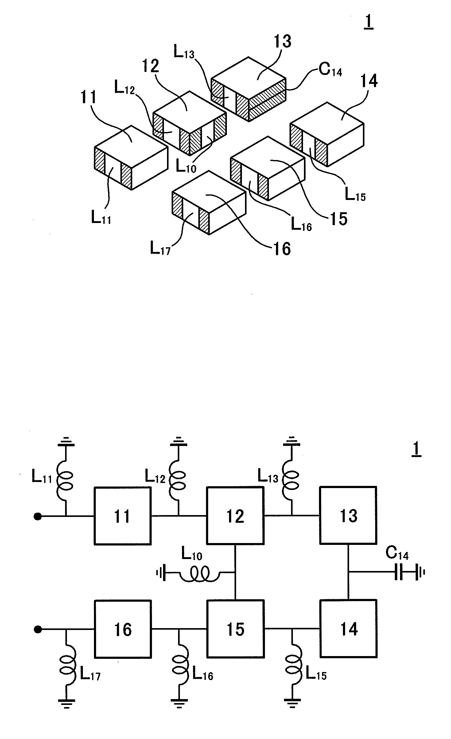
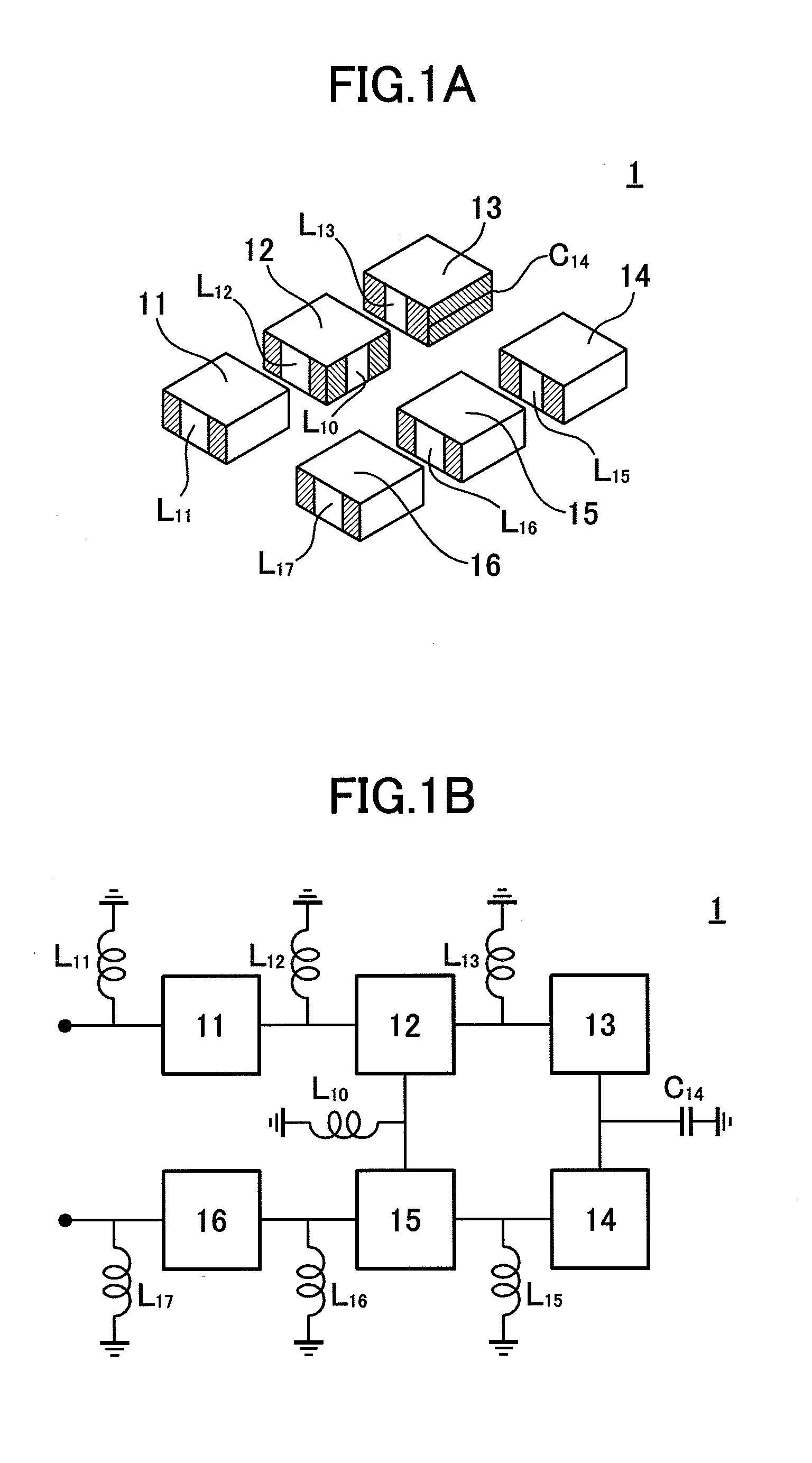
[0048]Using to the drawings, embodiments of the present invention will now be described below. FIG. 1A is an exploded perspective view of a dielectric waveguide filter according to the present invention, and FIG. 1B is an equivalent circuit diagram corresponding to FIG. 1A. As illustrated in FIGS. 1A and 1B, the dielectric waveguide filter 1 comprises six dielectric waveguide resonators 11 to 16 each having a rectangular parallelepiped-shaped dielectric block peripherally covered by a conductor film. The dielectric waveguide resonator 11 has an inductive window L11 for input, and the dielectric waveguide resonator 16 has an inductive window L17 for output. The dielectric waveguide resonators 11 to 13 are coupled in series through inductive windows L12, L13, and the dielectric waveguide resonators 14 to 16 are coupled in series through inductive windows L15, L16. A mutual coupling between the dielectric waveguide resonator 13 and the dielectric waveguide resonator 14 is established t...

second embodiment

[0053]FIG. 3A is an exploded perspective view of a dielectric waveguide filter according to the present invention. FIG. 3B is an explanatory detail diagram illustrating a part of the exploded perspective view of FIG. 3A, and FIG. 3C is an equivalent circuit diagram corresponding to FIG. 3A.

[0054]As illustrated in FIGS. 3A and 3B, the dielectric waveguide filter 3 comprises six dielectric waveguide resonators 31 to 36 each having a rectangular parallelepiped-shaped dielectric block peripherally covered by a conductor film, and a dielectric plate 37 peripherally covered by a conductor film.

[0055]The dielectric waveguide resonator 31 has an inductive window L31 for input, and the dielectric waveguide resonator 36 has an inductive window L37 for output. The dielectric waveguide resonators 31 to 33 are coupled in series through inductive windows L32, L33, and the dielectric waveguide resonators 34 to 36 are coupled in series through inductive windows L35, L36. The dielectric waveguide re...

third embodiment

[0072]FIG. 7A is an exploded perspective view of a dielectric waveguide filter according to the present invention, and FIG. 7B is an equivalent circuit diagram corresponding to FIG. 7A.

[0073]As illustrated in FIGS. 7A and 7B, the dielectric waveguide filter 7 has a main coupling path passing through dielectric waveguide resonators 71, 72, 73, 74, 75, 76, a first sub coupling path passing through the dielectric waveguide resonators 71, 72, 75, 76, and a second sub coupling path passing through the dielectric waveguide resonators 71, 76.

[0074]Even when there are two or more sub coupling paths as in the third embodiment, at least one capacitive coupling path may be provided on the main coupling paths, and a capacitive coupling path may be provided on one of the sub coupling paths. Further, the dielectric plate as illustrated in the second embodiment may be inserted in the capacitive coupling path.

[0075]As described above, in the dielectric waveguide filter of the present invention, a c...


PUM


Abstract

[OBJECT]It is an object to provide a dielectric waveguide filter with attenuation poles, which is capable of suppressing deterioration in a high band-side attenuation characteristic with respect to a low band-side attenuation characteristic.[SOLUTION]A dielectric waveguide filter comprises a plurality of dielectric waveguide resonators each having a rectangular parallelepiped-shaped dielectric block, periphery of which is covered by a conductor film. The dielectric waveguide resonators are configured to form a main coupling path, and a sub coupling path bypassing a part of the main coupling path. The part of the main coupling path bypassed by the sub coupling path includes at least one capacitive coupling path.

Description

TECHNICAL FIELD[0001]The present invention relates to a dielectric waveguide filter having a plurality of dielectric waveguide resonators coupled together.BACKGROUND ART[0002]In order allow wireless communication channels to be set adjacently to each other as close as possible so as to effectively utilize frequency resources, a base station for mobile phones or the like requires a bandpass filter having a steep attenuation characteristic for preventing inter-channel interference. If a bandpass filter using a small-size and lightweight dielectric waveguide resonator, called a “dielectric waveguide filter”, is used in place of a large and heavy metal cavity resonator, the base station can be reduced in size and weight. It also becomes possible to facilitate a reduction in cost of the base station.[0003]The dielectric waveguide filter is constructed by combining a plurality of dielectric waveguide resonators each having a dielectric block peripherally covered by a conductor film and pa...

Claims


Application Information

Patent Timeline
IPC IPC(8): H01P1/20H01P3/16
CPCH01P1/2084H01P7/10H01P1/2002H01P1/2088H01P1/20H01P5/08
Inventor ITO, KAZUHIRO
Owner MURATA MFG CO LTD
Learn More