
Apparatus for removal of docking plate in semiconductor equipment

Active Publication Date: 2012-09-20
MACRONIX INT CO LTD
View PDF3 Cites 0 Cited by
  • Summary
  • Abstract
  • Description
  • Claims
  • Application Information

AI Technical Summary

Benefits of technology

[0006]The original concept is to figure out a method for docking plate removal which can efficiently speed up the traditional hammer method and reduce any damage cost of the docking plate to ensure wafer processing schedule can be performed seamlessly without significant interruption during maintenance period. In addition, a stock and / or reordering of new docking plate which will add unexpected effect on smoothly designed clean procedure for semiconductor manufacturing equipment can be eliminated due to the simplified and reliable invention disclosed thereafter.
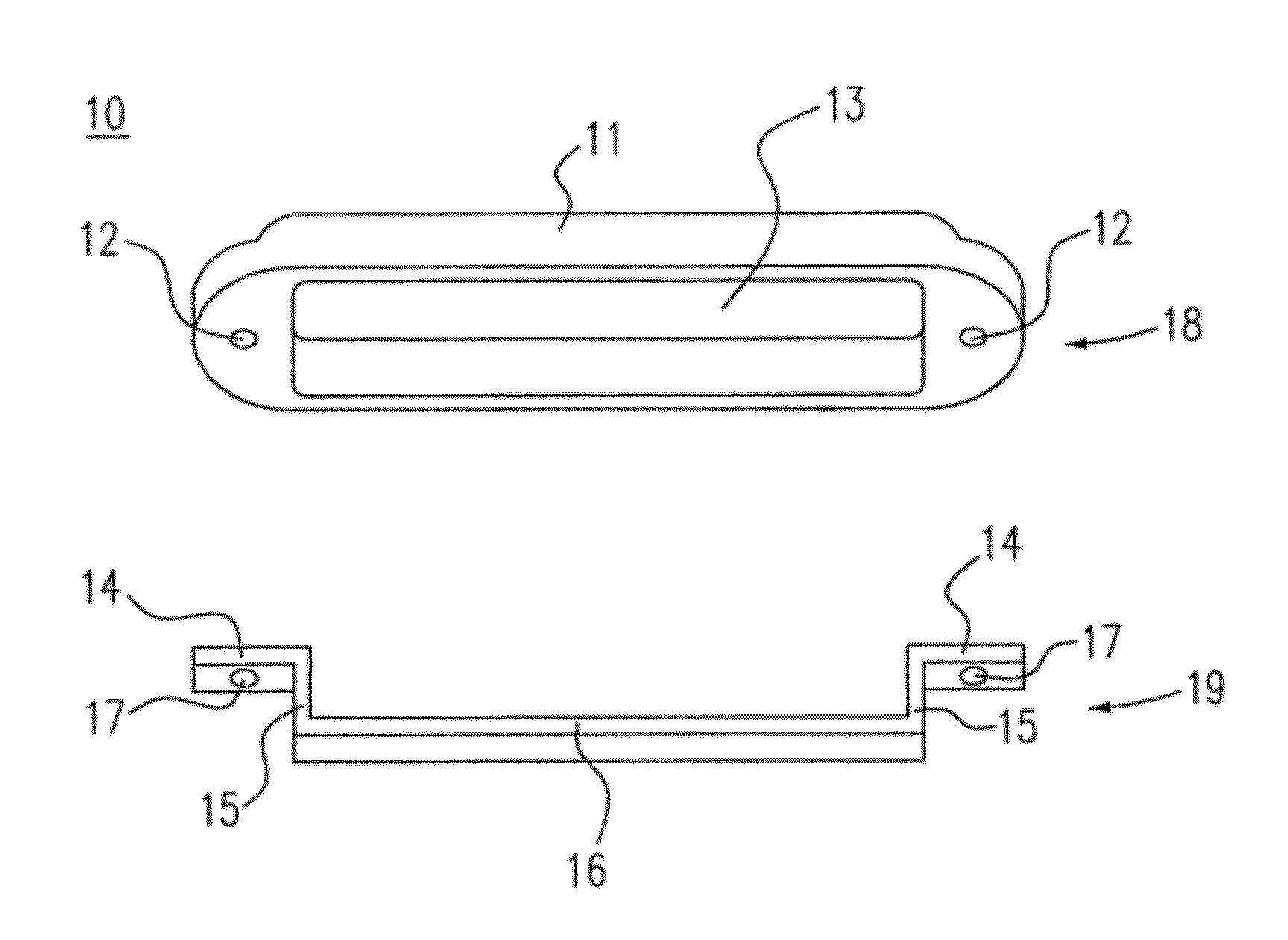
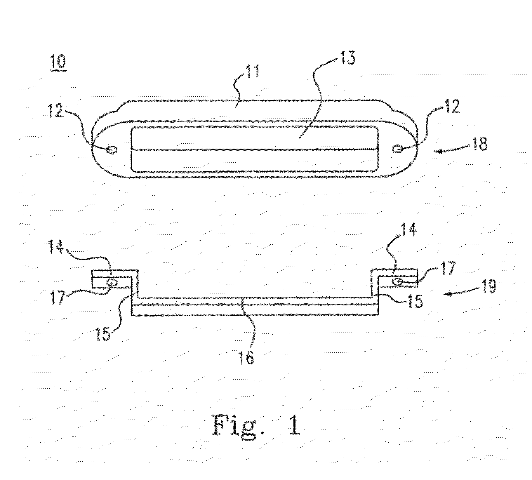
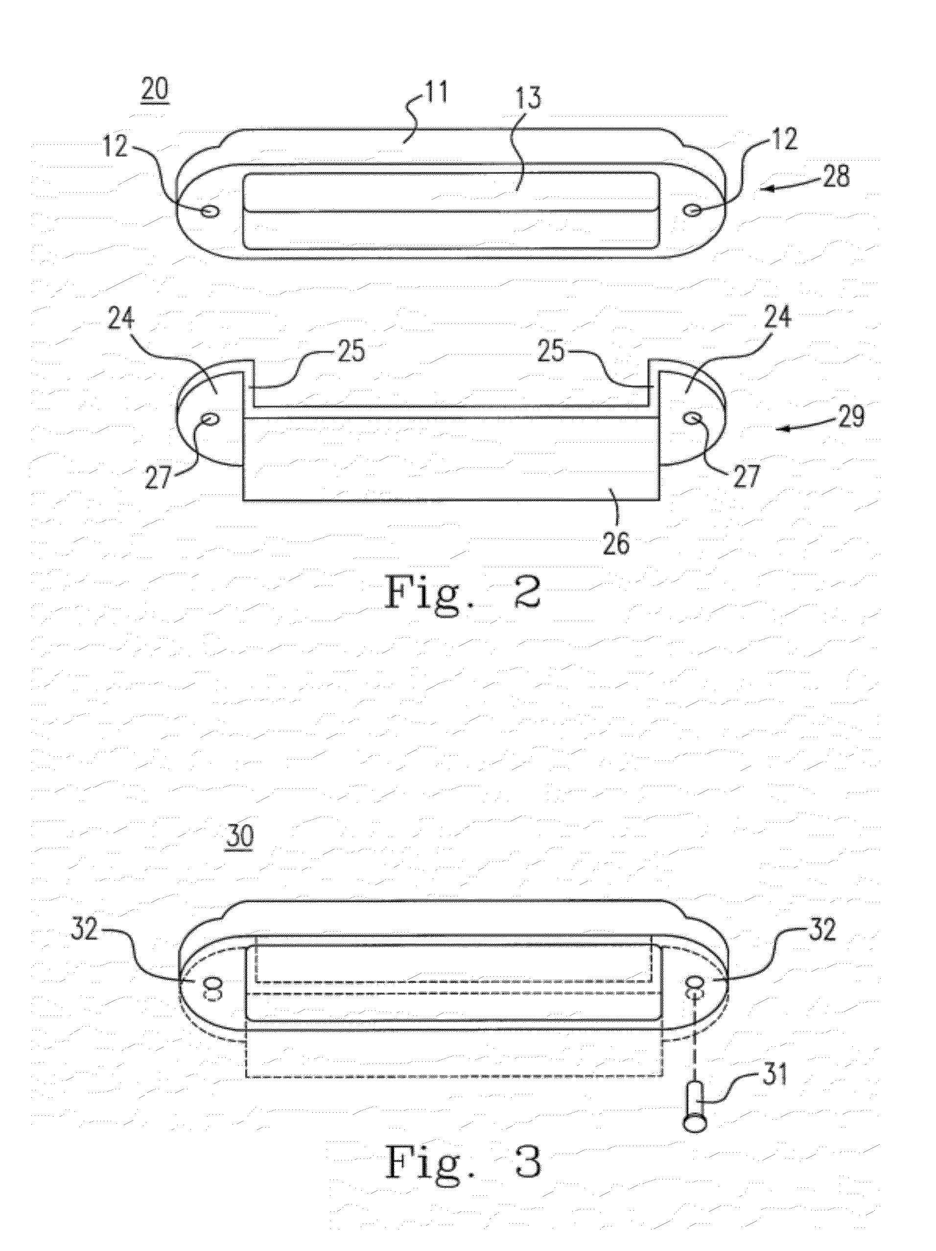
[0007]According to above thought, a docking plate combination for a semiconductor equipment, including: a docking plate base device; and a handle removably joined to the docking plate base device and causing the docking plate base device to be removed from the semiconductor equipment when the handle is joined to the docking plate base device.

Problems solved by technology

However, this manner is not only consuming significant time but is also easily to damage the docking plate which has a high cost in price and is not always available in the tool market due to a small amount of quantity in semiconductor equipment deployment.
For the requirement of continuous producing wafers in semiconductor industry, the above method will put in uncertainty interruption factor to tightly processing schedule and a consequence to semiconductor engineers, the method is apparently not applicable.
Furthermore, an equipment downtime which is ranged a couple of hours is needed to merely taking off the docking plate that is a required procedure to the replacement of docking O-ring.
Due to physical enforcement on the hammer, this is not only to say a waste of energy and but clearance of space for applying the force which will result in increasing complexity to redeploy all apparatuses for restart of the semiconductor equipment.
A high attention must be paid during this removal action, otherwise, damage to the docking plate will cause a beyond repaired condition.
And reordering the toll and a expenditure are unavoidable, while in the same time, a downtime for waiting the arrival of new docking plate is also harmful to intensive working tempo in semiconductor industry.

Method used


Image

  • Apparatus for removal of docking plate in semiconductor equipment
  • Apparatus for removal of docking plate in semiconductor equipment
  • Apparatus for removal of docking plate in semiconductor equipment

Examples


Embodiment Construction

[0027]The present invention will now be described more specifically with reference to the following embodiments. It is to be noted that the following descriptions of preferred embodiments of this invention are presented herein for purposes of illustration and description only; it is not intended to be exhaustive or to be limited to the precise form disclosed.

[0028]Please refer to FIGS. 1 and 4, the docking plate combination 10 in FIG. 1 is a connection between the neighboring chambers 41, 42 and can be inserted into and taken apart from the channel 43 in FIG. 4 by applying a pull force on the handle 16 of the combination 10. Care must be made with gently increasing the pull force with shaking left end and right end without causing permanent damage to the physical metal substance which is physical contact to the channel 43 surface of the semiconductor equipment. Once the docking plate combination 10 is removed from the channel 43 of semiconductor equipment, the docking O-ring can fur...


PUM


Abstract

The present invention relates to an apparatus for removal of docking plate, wherein comprising a docking plate base device; and a handle removably joined to the docking plate base device and causing the docking plate base device to be removed from the semiconductor equipment when the handle is joined to the docking plate base device.

Description

FIELD OF THE INVENTION[0001]The present invention relates to an apparatus for removal of docking plate, in particular an apparatus for removal of docking plate in semiconductor equipment.BACKGROUND OF THE INVENTION[0002]Semiconductor manufacturing engineering is a processing technology including plasma etching and deposition used for producing silicon wafers in which has a clean procedure must be performed to reduce equipment fault time by efficient removal of connecting apparatus including docking O-ring and docking plate. Therefore, engineers are trained to periodically stop the semiconductor running equipment, to remove all connecting apparatus and to clean all parts which contain pollution of article through the above etching and deposition process.[0003]With an example for taking apart of docking plate with hammer grasped by hand, the method is the traditional way to unload the docking plate and repeat tapping is necessary since the docking plate is tightly attached to the chan...

Claims


Application Information

Patent Timeline
IPC IPC(8): B23Q3/00
CPCH05K5/023
Inventor SUEN, BING-YI
Owner MACRONIX INT CO LTD
Learn More