Liquid crystal device and projection-type display apparatus

a liquid crystal device and display apparatus technology, applied in non-linear optics, instruments, optics, etc., can solve the problems of inability to cure, inability to reliably prevent aggregation of ionic impurities in image display regions, and inability to cause burn-in (discoloration) of images, etc., to achieve the effect of increasing the number of ionic impurities and easy to affect the quality of images

Active Publication Date: 2012-09-27
SEIKO EPSON CORP
View PDF3 Cites 10 Cited by
  • Summary
  • Abstract
  • Description
  • Claims
  • Application Information

AI Technical Summary

Benefits of technology

[0008]An advantage of some aspects of the invention is that it provides a liquid crystal device in which, regarding a peripheral electrode extending along a seal material, an ability of the peripheral electrode to trap ionic impurities from a region where display quality is easily affected by ionic impurities is increased, and a projection-type display apparatus including the liquid crystal device.
[0010]In this aspect of the invention, the peripheral electrode extending along the seal material in the peripheral region is provided in the element substrate, and a potential different from the common potential is applied to the peripheral electrode. Consequently, an electric field in a thickness direction of the liquid crystal layer is generated between the peripheral electrode and the common electrode. Therefore, even though ionic impurities infiltrating during liquid crystal injection, ionic impurities eluted from the seal material, and ionic impurities eluted from the sealing material are present in liquid crystals and the ionic impurities try to be aggregated in an end portion of the image display region due to driving of the liquid crystals, the ionic impurities are pulled into the peripheral electrode in the peripheral region or a portion of the common electrode opposing the peripheral electrode, and the pulled ionic impurities are stayed in the peripheral region while being aggregated therein. Here, according to the aspect of the invention, focusing on the fact that an ability of the peripheral electrode to trap ionic impurities is generally proportionate to the area of the peripheral electrode, the electrode width Wb of the portion of the peripheral electrode opposing the sealing material from which ionic impurities are more likely to be eluted is set to be greater than the electrode width Wa of the portions extending at other positions. Accordingly, the ionic impurities eluted from the sealing material can be efficiently pulled and stayed therein. Therefore, according to the aspect of the invention, it is difficult for the ionic impurities to be aggregated in the image display region, so that degradation of display quality caused by the ionic impurities rarely occurs.
[0011]According to the aspect of the invention, the peripheral electrode may employ a configuration in which a first portion which extends along a side where the sealing material is provided in the seal material, a second portion which opposes the first portion with the image display region interposed therebetween, a third portion which is provided between one ends of the first and second portions, and a fourth portion which opposes the third portion with the image display region interposed therebetween are provided and the first portion has the electrode width Wb. In this configuration, since the entirety of the first portion extending along the portion where the sealing material is provided extends with the electrode width Wb which is large, ionic impurities eluted from the sealing material can be efficiently pulled and stayed therein.
[0012]According to the aspect of the invention, it is preferable that from the second, third, and fourth portions in the peripheral electrode, the portion extending in a region where the peripheral region has a large width extends with the electrode width Wa, and the portion extending in a region where the peripheral region has a small width extends with an electrode width Wc that is greater than the electrode width Wa. For example, the second portion extends with the electrode width Wc, and the third and fourth portions extend with the electrode width Wa. In this configuration, since the electrode width of the peripheral electrode provided at a point where the interval between the seal material and the image display region is narrow is large, infiltration of ionic impurities eluted from the seal material into the image display region can be effectively prevented.
[0013]According to the aspect of the invention, a configuration in which the electrode width We is equal to the electrode width Wb may be employed. In this configuration, since the electrode width of the peripheral electrode provided at a point where the interval between the seal material and the image display region is narrow is large, infiltration of ionic impurities eluted from the seal material into the image display region can be effectively prevented.
[0014]The aspect of the invention is effective when being applied to a case where an alignment film is an inorganic alignment film, and a nematic liquid crystal compound with negative dielectric anisotropy is used in the liquid crystal layer. The inorganic alignment film is more likely to adsorb ionic impurities. However, according to the aspect of the invention, even in the case where the alignment film is used, aggregation of ionic impurities in the image display region can be reliably prevented. In addition, in the case where the nematic liquid crystal compound with negative dielectric anisotropy is used in the liquid crystal layer, since liquid crystal molecules rotate about a point in a longitudinal direction, ionic impurities are easily gathered in a specific point and thus deterioration of images easily occurs. However, according to the aspect of the invention, even in the case where the nematic liquid crystal compound with negative dielectric anisotropy is used, aggregation of ionic impurities in the image display region can be reliably prevented.

Problems solved by technology

In such a liquid crystal device, when ionic impurities infiltrating during liquid crystal injection or ionic impurities eluted from the seal material are aggregated in the image display region by driving the liquid crystal device, degradation of display quality such as burn-in (discoloration) of an image is caused.
However, in the configuration described in JP-A-2008-58497, consideration for a structure unique to the liquid crystal device is not sufficiently made, so that there is a problem in that aggregation of ionic impurities in the image display region cannot be reliably prevented.
Contrary to this, a sealing material is cured after the liquid crystal material is sealed and thus cannot be cured under appropriate conditions for either light curing or thermal curing from the viewpoint of prevention of deterioration of the liquid crystal material.
However, the peripheral electrodes described in JP-A-2008-58497 cannot reliably pull the ionic impurities generated from the sealing material so as to be stayed therein.
Therefore, according to the aspect of the invention, it is difficult for the ionic impurities to be aggregated in the image display region, so that degradation of display quality caused by the ionic impurities rarely occurs.
In addition, in the case where the nematic liquid crystal compound with negative dielectric anisotropy is used in the liquid crystal layer, since liquid crystal molecules rotate about a point in a longitudinal direction, ionic impurities are easily gathered in a specific point and thus deterioration of images easily occurs.

Method used


Image

  • Liquid crystal device and projection-type display apparatus
  • Liquid crystal device and projection-type display apparatus
  • Liquid crystal device and projection-type display apparatus

Examples


first embodiment

Overall Configuration

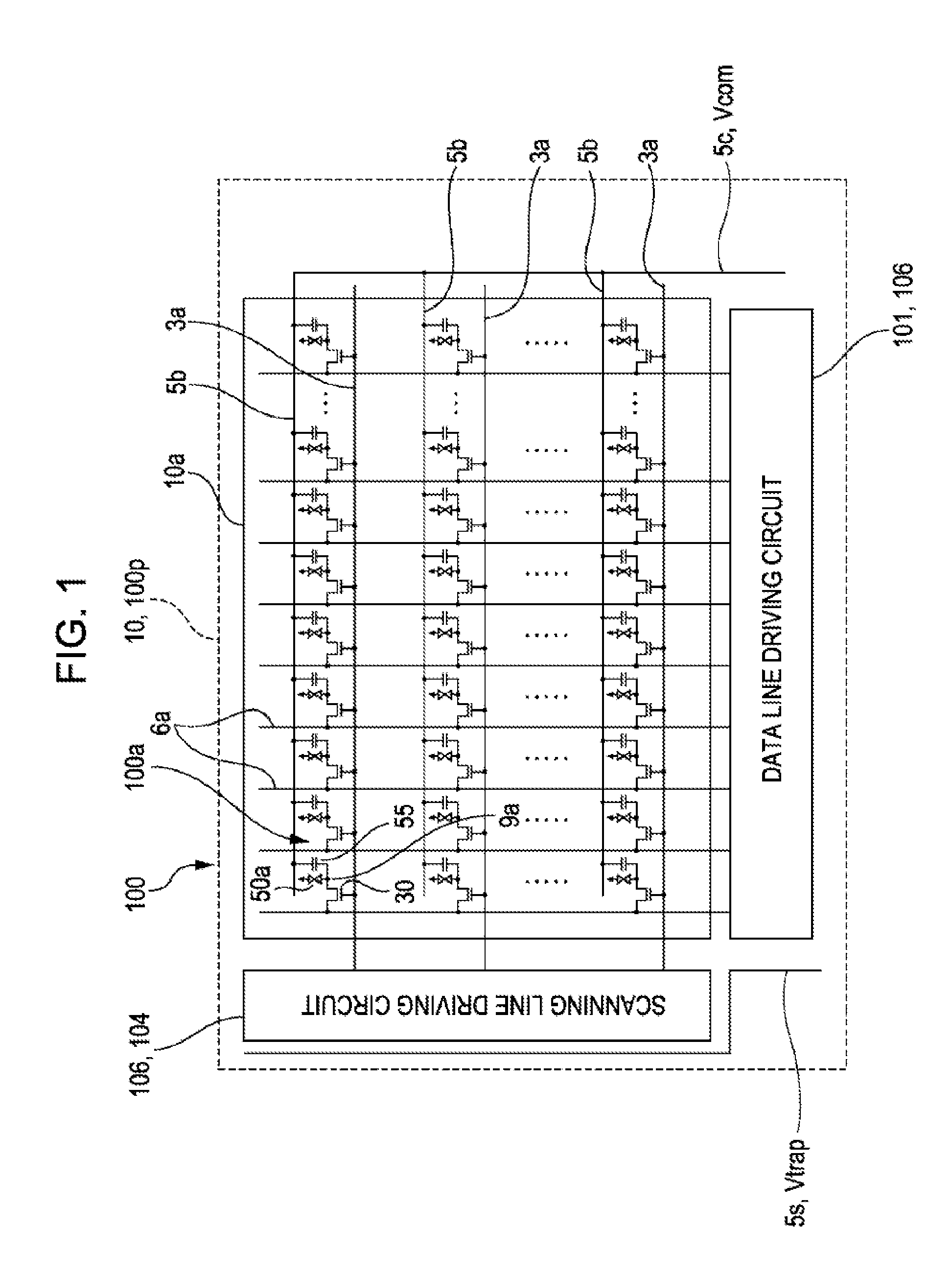
[0029]FIG. 1 is a block diagram illustrating an electrical configuration of a liquid crystal device to which an embodiment of the invention is applied. In addition, FIG. 1 is a block diagram illustrating only the electrical configuration and does not illustrate shapes of wires and electrodes, extension directions, layouts, and the like.

[0030]In FIG. 1, a liquid crystal device 100 has a liquid crystal panel 100p in a TN (Twisted Nematic) mode or a VA (Vertical Alignment) mode, and the liquid crystal panel 100p includes an image display region 10a (image display region) having a plurality of pixels 100a arranged in a matrix form at the center region. In the liquid crystal panel 100p, in an element substrate 10 (see FIGS. 2A and 2B and the like) described later, a plurality of data lines 6a and a plurality of scanning lines 3a extend vertically and horizontally inside the image display region 10a, and pixels 100a are configured at positions corresponding to the int...

second embodiment

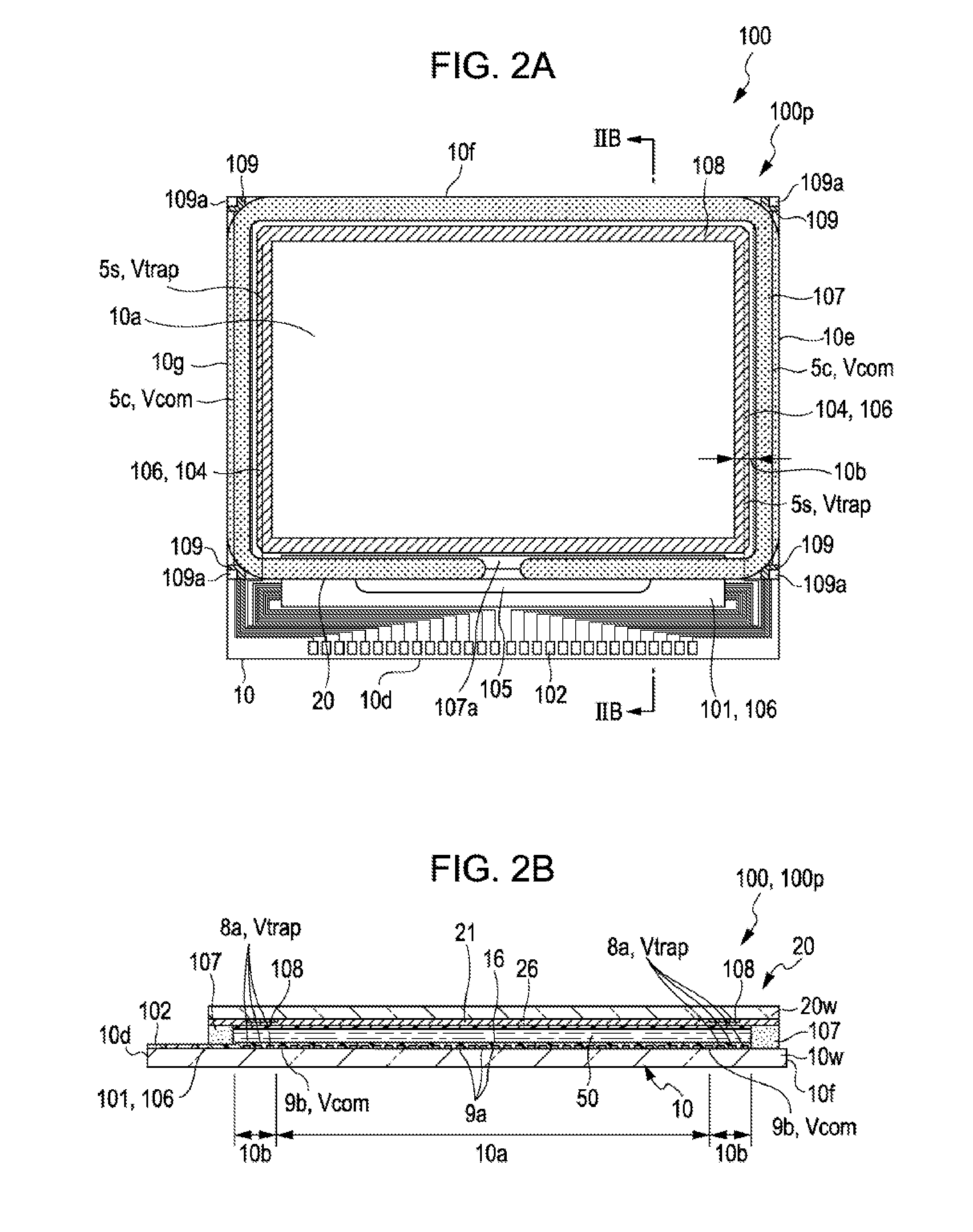
[0074]FIG. 7 is a diagram illustrating the peripheral electrode 8a formed on the element substrate 10 of the liquid crystal device 100 according to a second embodiment of the invention. In addition, in FIG. 7, the number of the pixel electrodes 9a, the dummy pixel electrodes 9b, and the like is reduced for illustration. Since the basic configuration of this embodiment is the same as that of the first embodiment, like elements that are common are denoted by like reference numerals, and description thereof will be omitted.

[0075]In the first embodiment, all the second, third, and fourth portions 8a2, 8a3, and 8a4 have the electrode width Wa. However, in this embodiment, as illustrated in FIG. 7, a configuration is employed in which, from among the second, third, and fourth portions 8a2, 8a3, and 8a4, the portions that extend in a region where the peripheral region 10b has a large width extend with the electrode width Wa, and the portions that extend in a region where the peripheral reg...

third embodiment

[0080]FIG. 8 is a diagram illustrating the peripheral electrode 8a formed on the element substrate 10 of the liquid crystal device 100 according to a third embodiment of the invention. In addition, in FIG. 8, the number of the pixel electrodes 9a, the dummy pixel electrodes 9b, and the like is reduced for illustration. Since the basic configuration of this embodiment is the same as that of the first embodiment, like elements that are common are denoted by like reference numerals, and description thereof will be omitted.

[0081]In the second embodiment, the electrode width Wa of the third and fourth portions 8a3 and 8a4, the electrode width Wb of the first portion 8a1, and the electrode width Wc of the second portion 8a2 have the following relationship of the electrode width Wa8a1 and the electrode width Wc of the second portion 8a2 are equal to each other. That is, the electrode width Wa of the third and fourth portions 8a3 and 8a4, the electrode width Wb of the first portion 8a1, and...


PUM

PropertyMeasurementUnit
width Waaaaaaaaaaa
width Waaaaaaaaaaa
widthaaaaaaaaaa

Abstract

In an element substrate of a liquid crystal device, in a peripheral region interposed between an image display region and a seal material, a peripheral electrode to which a potential is applied for trapping ionic impurities which is different from a common potential applied to a dummy pixel electrode or the like is formed. In the peripheral electrode, an electrode width of a first portion opposing a sealing material provided at a liquid crystal injection opening of the seal material is set to be greater than electrode widths of the other portions.

Description

BACKGROUND[0001]1. Technical Field[0002]The present invention relates to a liquid crystal device in which liquid crystals are held between a pair of substrates, and a projection-type display apparatus which uses the liquid crystal device as a light valve.[0003]2. Related Art[0004]In a liquid crystal device, an element substrate provided with an image display region having a plurality of pixel electrodes arranged on one surface side and a counter substrate provided with a common electrode to which a common potential is applied are bonded to each other by a seal material, and a liquid crystal layer is held in a region surrounded by the seal material between the element substrate and the counter substrate. In order to manufacture the liquid crystal device, first, when the seal material is applied to the element substrate in a frame form, a broken portion is provided, and after the element substrate and the counter substrate are overlapped with each other via the seal material, the seal...

Claims


Application Information

Patent Timeline
Patent Type & Authority Applications(United States)
IPC IPC(8): G02F1/13357G02F1/1343
CPCG02F1/1333G02F2001/133388G02F2001/133337G02F1/134336G02F1/133337G02F1/133388
Inventor HARA, HIROYUKIYOKOTA, TOMOKI
Owner SEIKO EPSON CORP
Why Eureka
Try Eureka